PW567EA Datasheet
PW567EA Datasheet (UNIKC)
UNIKC
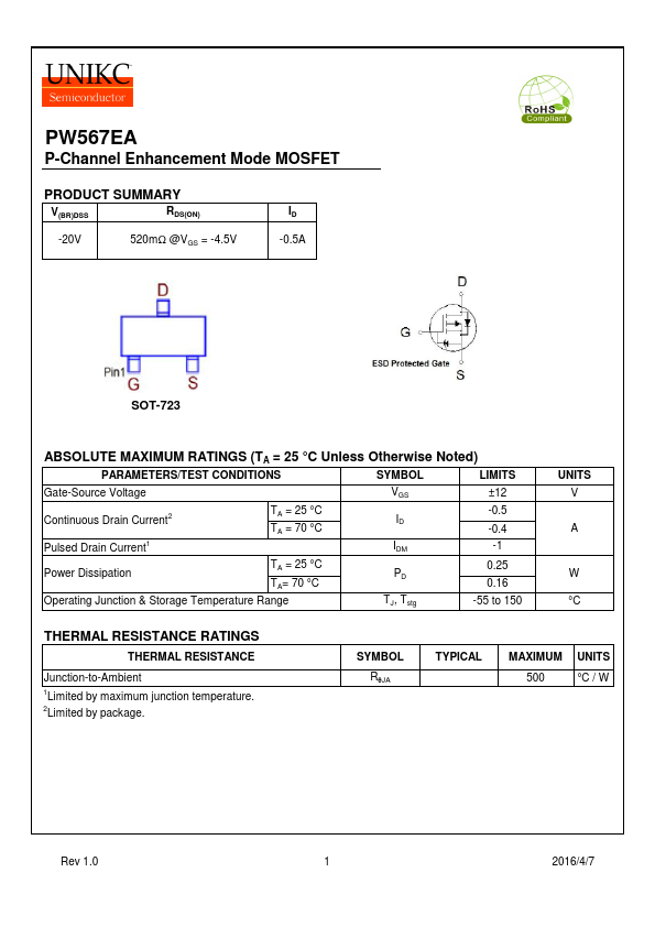
PW567EA P-Channel Enhancement Mode MOSFET PRODUCT SUMMARY V(BR)DSS RDS(ON) -20V 520mΩ @VGS = -4.5V ID -0.5A SOT-723 ABSOLUTE MAXIMUM RATINGS (TA = 25 °C Unless Otherwise Noted) PARAMETERS/TES.
VGS, ID = -250mA VDS = 0V, VGS = ±12V -20 -0.4 -0.96 -1.2 ±30 Zero Gate Voltage Drain Current IDSS VDS = -16V, VGS = 0V VDS = -10V, VGS = 0V , TJ = 75 °C -1 -10 Drain-Source On-State Resistance1 Forward Transconductance1 RDS(ON) gfs VGS = -4.5V, ID = -450mA VGS = -2.5V, ID = -100mA VDS = -5V.
PW567EA Datasheet (NIKO-SEM)
NIKO-SEM
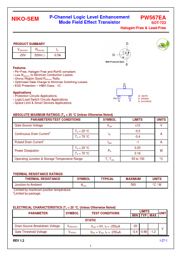
NIKO-SEM P-Channel Logic Level Enhancement Mode Field Effect Transistor PW567EA SOT-723 Halogen-Free & Lead-Free PRODUCT SUMMARY V(BR)DSS RDS(ON) -20V 520mΩ ID -0.5A Features • Pb−Free, Halo.
* Pb
*Free, Halogen Free and RoHS compliant.
* Low RDS(on) to Minimize Conduction Losses.
* Ohmic Region Good RDS(on) Ratio.
* Optimized Gate Charge to Minimize Switching Losses.
* ESD Protection
* HBM Class : 1C.
Applications
* Protection Circuits Applications.
* Logic/Load Switch Circuits Applicati.