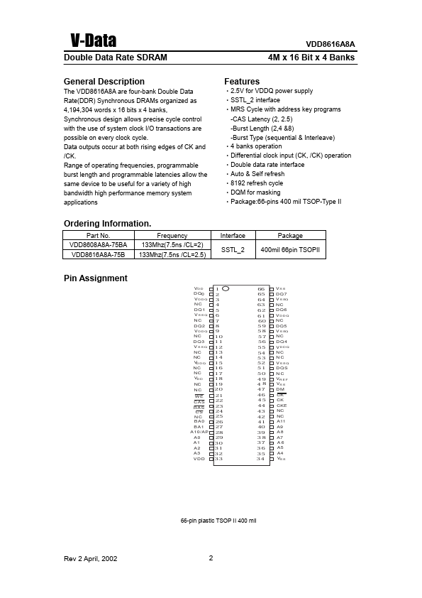
Datasheet4U Logo Datasheet4U.com

VDD8616A8A - DOUBLE DATA RATE SDRAM

Download the VDD8616A8A datasheet PDF. This datasheet also covers the VDD8616A8A-A variant, as both devices belong to the same double data rate sdram family and are provided as variant models within a single manufacturer datasheet.

General Description

The VDD8616A8A are four-bank Double Data Rate(DDR) Synchronous DRAMs organized as 4,194,304 words x 16 bits x 4 banks, Synchronous design allows precise cycle control with the use of system clock I/O transactions are possible on every clock cycle.

Key Features

  • 2.5V for VDDQ power supply.
  • SSTL_2 interface.
  • MRS Cycle with address key programs -CAS Latency (2, 2.5) -Burst Length (2,4 &8) -Burst Type (sequential & Interleave).
  • 4 banks operation.
  • Differential clock input (CK, /CK) operation.
  • Double data rate interface.
  • Auto & Self refresh.
  • 8192 refresh cycle.
  • DQM for masking.
  • Package:66-pins 400 mil TSOP-Type II Ordering Information. Part No. VDD8608A8A-75BA VDD8616A8A-75B Fr.

📥 Download Datasheet

Note: The manufacturer provides a single datasheet file (VDD8616A8A-A-Data.pdf) that lists specifications for multiple related part numbers.

Datasheet Details

Part number VDD8616A8A
Manufacturer A-Data
File Size 205.96 KB
Description DOUBLE DATA RATE SDRAM
Datasheet download datasheet VDD8616A8A Datasheet

Full PDF Text Transcription (Reference)

The following content is an automatically extracted verbatim text from the original manufacturer datasheet and is provided for reference purposes only.

View original datasheet text
V-Data Revision History Revision 1 ( Dec. 2001 ) 1.Fister release. VDD8616A8A Revision 2 ( Apr. 2002 ) 1. Changed module current specification. 2. Add Performance range. 3. Changed AC Characteristics. 4. Changed typo size on module PCB in package dimensions. Rev 2 April, 2002 1 V-Data Double Data Rate SDRAM General Description The VDD8616A8A are four-bank Double Data Rate(DDR) Synchronous DRAMs organized as 4,194,304 words x 16 bits x 4 banks, Synchronous design allows precise cycle control with the use of system clock I/O transactions are possible on every clock cycle. Data outputs occur at both rising edges of CK and /CK.