ACE3401D
ACE3401D is P-Channel Enhancement Mode Field Effect Transistor manufactured by ACE Technology.
P-Channel Enhancement Mode Field Effect Transistor
Description This device is particularly suited for low voltage application such as portable equipment, power management and other battery powered circuits, and low in-line power dissipation are needed in a very small outline surface mount package Excellent thermal and electrical capabilities.
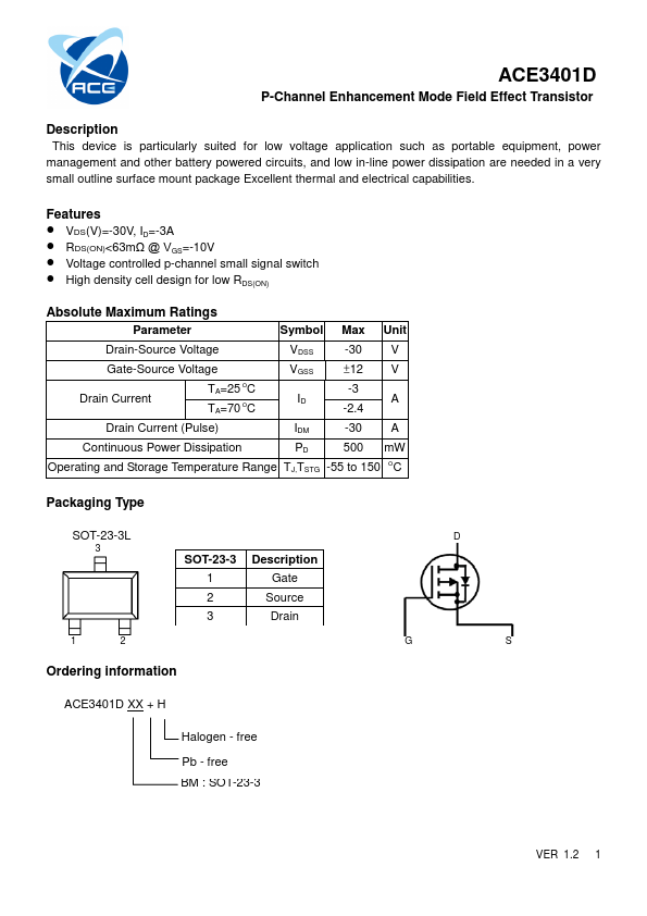
Features
- VDS(V)=-30V, ID=-3A
- RDS(ON)<63mΩ @ VGS=-10V
- Voltage controlled p-channel small signal switch
- High density cell design for low...