Datasheet4U Logo Datasheet4U.com

A67P0636 - (A67P0636 / A67P1618) Pipelined ZeBL SRAM

Download the A67P0636 datasheet PDF. This datasheet also covers the A67P1618 variant, as both devices belong to the same (a67p0636 / a67p1618) pipelined zebl sram family and are provided as variant models within a single manufacturer datasheet.

Description

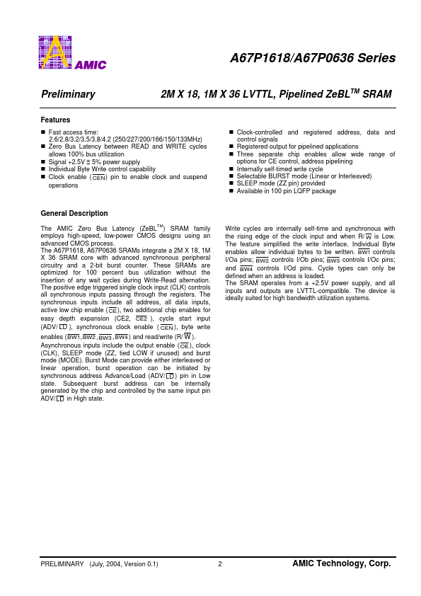
The AMIC Zero Bus Latency (ZeBLTM) SRAM family employs high-speed, low-power CMOS designs using an advanced CMOS process.

The A67P1618, A67P0636 SRAMs integrate a 2M X 18, 1M X 36 SRAM core with advanced synchronous peripheral circuitry and a 2-bit burst counter.

Features

  • Fast access time: 2.6/2.8/3.2/3.5/3.8/4.2 (250/227/200/166/150/133MHz) Zero Bus Latency between READ and WRITE cycles allows 100% bus utilization Signal +2.5V ± 5% power supply Individual Byte Write control capability Clock enable ( CEN ) pin to enable clock and suspend operations Clock-controlled and registered address, data and control signals Registered output for pipelined.

📥 Download Datasheet

Note: The manufacturer provides a single datasheet file (A67P1618_AMICTechnology.pdf) that lists specifications for multiple related part numbers.

Datasheet Details

Part number A67P0636
Manufacturer AMIC Technology
File Size 296.38 KB
Description (A67P0636 / A67P1618) Pipelined ZeBL SRAM
Datasheet download datasheet A67P0636 Datasheet

Full PDF Text Transcription (Reference)

The following content is an automatically extracted verbatim text from the original manufacturer datasheet and is provided for reference purposes only.

View original datasheet text
www.DataSheet4U.com A67P1618/A67P0636 Series Preliminary Document Title 2M X 18, 1M X 36 LVTTL, Pipelined ZeBLTM SRAM Revision History Rev. No. 0.0 0.1 2M X 18, 1M X 36 LVTTL, Pipelined ZeBLTM SRAM History Initial issue Error Correction: delete BWE pin in block diagram Issue Date March 25, 2004 August 6, 2004 Remark Preliminary PRELIMINARY (July, 2004, Version 0.1) AMIC Technology, Corp. A67P1618/A67P0636 Series Preliminary Features Fast access time: 2.6/2.8/3.2/3.5/3.8/4.2 (250/227/200/166/150/133MHz) Zero Bus Latency between READ and WRITE cycles allows 100% bus utilization Signal +2.
Published: |