PI3012A
PI3012A is 300DPI CIS Sensor Chip manufactured by AMI SEMICONDUCTOR.
Description
:
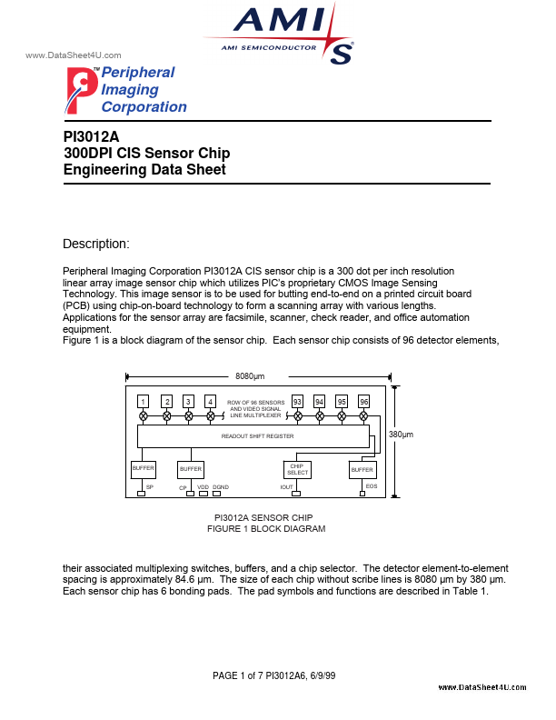
Peripheral Imaging Corporation PI3012A CIS sensor chip is a 300 dot per inch resolution linear array image sensor chip which utilizes PIC’s proprietary CMOS Image Sensing Technology. This image sensor is to be used for butting end-to-end on a printed circuit board (PCB) using chip-on-board technology to form a scanning array with various lengths. Applications for the sensor array are facsimile, scanner, check reader, and office automation equipment. Figure 1 is a block diagram of the sensor chip. Each sensor chip consists of 96 detector elements,
8080µm
1 2 3 4
ROW OF 96 SENSORS AND VIDEO SIGNAL LINE MULTIPLEXER
READOUT SHIFT REGISTER
380µm
BUFFER
BUFFER CP VDD DGND
CHIP SELECT IOUT
BUFFER EOS
PI3012A SENSOR CHIP FIGURE 1 BLOCK DIAGRAM their associated multiplexing switches, buffers, and a chip selector. The detector element-to-element spacing is approximately 84.6 µm. The size of each chip without scribe lines is 8080 µm by 380 µm. Each sensor chip has 6 bonding pads. The pad symbols and functions are described in Table 1.
PAGE 1 of 7 PI3012A6, 6/9/99
..
SYMBOL SP CP VDD DGND IOUT EOS
FUNCTION Start Pulse: Input to start the line scan. Clock Pulse: Input to clock the Shift Register. Positive Supply: +5 volt supply connected to substrate. Digital Ground: Connection topside mon. Signal Current Output: Output for video signal current End of Scan Pulse: Output from the shift register at end of scan. Table 1. Pad Symbols and Functions
Bonding pad layout diagram:
8080 µm
SENSOR DIE
380µm
IOUT B1 W1 EOS
NOTE: ALL PAD OPENNINGS ARE 140 X 80 µm EXCEPT FOR THE TEST PADS, WHICH ARE 80 X 80 µm.
SP CP VDD VSS IOUT EOS W C B E B1 W1
FUNCTION
START INPUT CLOCK INPUT + 5 VOLT SUPPLY GROUND VIDEO SIGNAL OUT SCAN OUTPUT TP TP TP TP TP TP
30 30 30 30 30 30 30 30 30 30 30 30
742.5 2767.0 3124.5 3419.0 5095.5 7000.1 1162.5 1312.5 1658.0 1807.0 5407.0 5672.0
NOTES: 1. THE DRAWING IS NOT TO...