PI3034A
PI3034A is 200DPI CIS Sensor Chip manufactured by AMI SEMICONDUCTOR.
Description
:
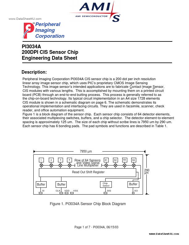
Peripheral Imaging Corporation PI3034A CIS sensor chip is a 200 dot per inch resolution linear array image sensor chip, which uses PIC’s proprietary CMOS Image Sensing Technology. This image sensor’s intended applications are to fabricate Contact Image Sensor, CIS modules with various lengths. This is acplished by mounting them on a printed circuit board (PCB) through an end-to-end butting process. This process is generally referred to as the chip-on-board technology. Its typical circuit implementation in an A4 size 1728 elements CIS module is shown in a schematic diagram on page 6. The schematic demonstrates its operational implementation and interfacing circuits. They are used in facsimile, scanner, check reader, and office automation equipment. Figure 1 is a block diagram of the sensor chip. Each sensor chip consists of 64 detector elements, their associated multiplexing switches, buffers, and a chip selector. The detector element-to-element spacing is approximately 125 um. The size of each chip without scribe lines is 7950 um by 290 um. Each sensor chip has 6 bonding pads. The pad symbols and functions are described in Table 1.
7950 µm
1 2 3 4
Row of 64 Sensors and Video Signal Line Multiplexer Read Out Shift Register
290 µm
Buffer
Buffer
CLK VDD VSS
Chip Select SIG
Buffer
Figure 1. PI3034A Sensor Chip Block Diagram
Page 1 of 7
- PI3034A, 06/15/03
..
SYMBOL SI CLK VDD VSS SIG SO
FUNCTION Start Pulse: Input to start the line scan. Clock Pulse: Input to clock the Shift Register. Positive Supply: +5 volt supply connected to substrate. Digital Ground: Connection topside mon. Signal Current Output: Output for video signal current End of Scan Pulse: Output from the shift register at end of scan.
Table 1. Pad Symbols and Functions Bonding pad layout diagram:
Figure 2 shows the bonding pad locations for PI3034A Sensor Chip relative to the lower left corner of the die.
7950 µm SENSOR DIE
290 µm SIG...