Features
• Low-voltage and Standard-voltage Operation
– 1.8 (VCC = 1.8V to 5.5V)
• Internally Organized as 32,768 x 8
• Two-wire Serial Interface
• Schmitt Trigger, Filtered Inputs for Noise Suppression
• Bidirectional Data Transfer Protocol
• 1 MHz (5.0V, 2.7V, 2.5V), and 400 kHz (1.8V) Compatibility
• Write Protect Pin for Hardware and Software Data Protection
• 64-byte Page Write Mode (Partial Page Writes Allowed)
• Self-timed Write Cycle (5 ms Max)
• High Reliability
– Endurance: One Million Write Cycles
– Data Retention: 40 Years
• Lead-free/Halogen-free Devices Available
• 8-lead JEDEC PDIP, 8-lead JEDEC SOIC, EIAJ SOIC, 8-lead Ultra Thin Small Array
Package (SAP), 8-lead TSSOP, and 8-ball dBGA2 Packages
• Die Sales: Wafer Form, Waffle Pack and Bumped Wafers
Two-wire Serial
EEPROM
256K (32,768 x 8)
AT24C256B
Description
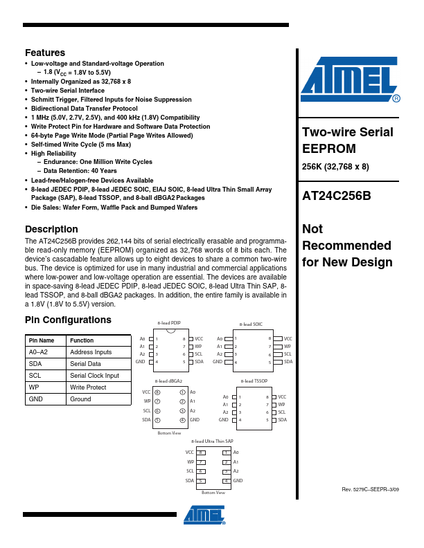
The AT24C256B provides 262,144 bits of serial electrically erasable and programma-
ble read-only memory (EEPROM) organized as 32,768 words of 8 bits each. The
device’s cascadable feature allows up to eight devices to share a common two-wire
bus. The device is optimized for use in many industrial and commercial applications
where low-power and low-voltage operation are essential. The devices are available
in space-saving 8-lead JEDEC PDIP, 8-lead JEDEC SOIC, 8-lead Ultra Thin SAP, 8-
lead TSSOP, and 8-ball dBGA2 packages. In addition, the entire family is available in
a 1.8V (1.8V to 5.5V) version.
Not
Recommended
for New Design
Pin Configurations
8-lead PDIP
8-lead SOIC
Pin Name
A0–A2
SDA
SCL
WP
GND
Function
Address Inputs
Serial Data
Serial Clock Input
Write Protect
Ground
A0
A1
A2
GND
1
2
3
4
8 VCC
A0
7 WP
A1
6 SCL
A2
5 SDA GND
1
2
3
4
8 VCC
7 WP
6 SCL
5 SDA
8-lead dBGA2
VCC 8
WP 7
SCL 6
SDA 5
1 A0
2 A1
3 A2
4 GND
8-lead TSSOP
A0
A1
A2
GND
1
2
3
4
8 VCC
7 WP
6 SCL
5 SDA
Bottom View
8-lead Ultra Thin SAP
VCC 8
WP 7
SCL 6
SDA 5
1 A0
2 A1
3 A2
4 GND
Bottom View
Rev. 5279C–SEEPR–3/09