AT25F512A Datasheet Text
Features
- Serial Peripheral Interface (SPI) patible
- Supports SPI Modes 0 (0,0) and 3 (1,1)
- Datasheet Describes 0 Operation
- 33 MHz Clock Rate
- Byte Mode and 128-byte Page Mode for Program Operations
- Sector Architecture:
- Two Sectors with 32K Bytes Each
- 256 Pages per Sector
- Product Identification Mode
- Low-voltage Operation
- 2.7 (VCC = 2.7 to 3.6V)
- Sector Write Protection
- Write Protect (WP) Pin and Write Disable Instructions for both Hardware and Software
Data Protection
- Self-timed Program Cycle (75 µs/byte typical)
- Self-timed Sector Erase Cycle (1 second/sector typical)
- Single Cycle Reprogramming (Erase and Program) for Status Register
- High Reliability
- Endurance: 10,000 Write Cycles Typical
- Data Retention: 20 Years
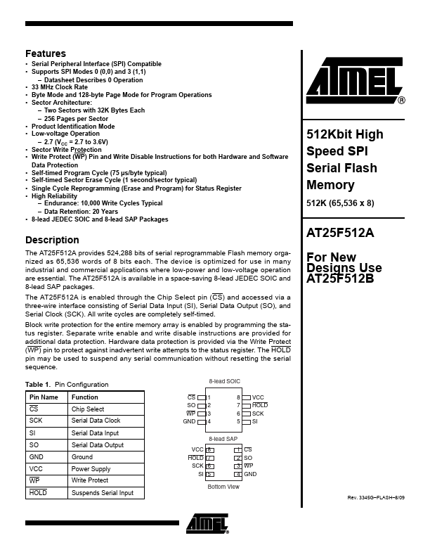
- 8-lead JEDEC SOIC and 8-lead SAP Packages
Description
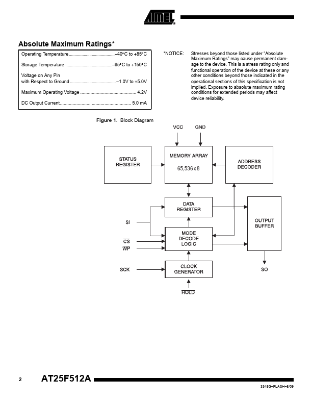
The AT25F512A provides 524,288 bits of serial reprogrammable Flash memory organized as 65,536 words of 8 bits each. The device is optimized...