• Part: MGA-30989
  • Description: High Linearity Gain Block
  • Manufacturer: Avago Technologies
  • Size: 364.59 KB
Download MGA-30989 Datasheet PDF
Avago Technologies
MGA-30989
MGA-30989 is High Linearity Gain Block manufactured by Avago Technologies.
Description 
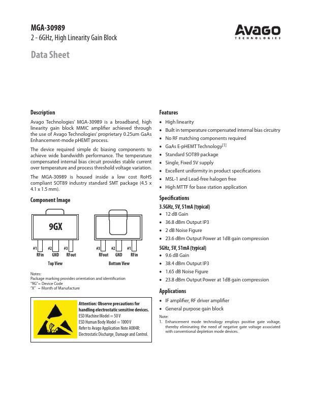
Avago Technologies’ MGA-30989 is a broadband, high linearity gain block MMIC amplifier achieved through the use of Avago Technologies’ proprietary 0.25um Ga As Enhancement-mode p HEMT process. The device required simple dc biasing ponents to achieve wide bandwidth performance. The temperature pensated internal bias circuit provides stable current over temperature and process threshold voltage variation. The MGA-30989 is housed inside a low cost Ro HS pliant SOT89 industry standard SMT package (4.5 x 4.1 x 1.5 mm). ponent Image 9GX #1 #2 #3 RFin GND RFout Top View #3 #2 #1 RFout GND RFin Bottom View Notes: Package marking provides orientation and identification “9G”= Device Code “X” = Month of Manufacture Attention: Observe precautions for handling electrostatic sensitive devices. ESD Machine Model = 50 V ESD Human Body Model = 1000 V Refer to Avago Application Note A004R: Electrostatic Discharge, Damage and Control. Features x High linearity x Built in temperature pensated internal bias circuitry x No RF matching ponents required x Ga As E-p HEMT Technology[1] x Standard SOT89 package x Single, Fixed 5V supply x Excellent uniformity in product specifications x MSL-1 and Lead-free halogen free x High MTTF for base station application Specifications 3.5GHz, 5V, 51m A (typical) x 12 d B Gain x 36.8 d Bm Output IP3 x 2 d B Noise Figure x 23.6 d Bm Output Power at 1d B gain pression 5GHz, 5V, 51m A (typical) x 9.6 d B Gain x 38.4 d Bm Output IP3 x 1.65 d B Noise Figure x 23.8 d Bm Output Power at 1d B gain pression Applications x IF amplifier, RF driver amplifier x General purpose gain block Note: 1. Enhancement mode technology employs positive gate voltage, thereby eliminating the need of negative gate voltage associated with conventional depletion mode devices. Absolute Maximum Rating[1] TA=25°C Symbol Vdd,max Pin,max Pdiss Tj,MAX TSTG Parameter Device Voltage, RF output to ground CW RF Input Power Total Power Dissipation [3] Junction Temperature Storage...