Download AP50T10AGP-HF-3 Datasheet PDF
Advanced Power Electronics Corp
AP50T10AGP-HF-3
AP50T10AGP-HF-3 is N-CHANNEL ENHANCEMENT MODE POWER MOSFET manufactured by Advanced Power Electronics Corp.
Description 
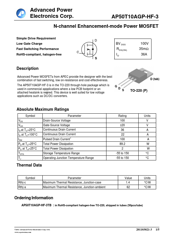
Advanced Power MOSFETs from APEC provide the designer with the best bination of fast switching, low on-resistance and cost-effectiveness. The AP50T10AGP-HF-3 is in the TO-220 through-hole package which is used in mercial appplications where a low PCB footprint or an attached heatsink is required. This device is well suited for low voltage applications such as DC/DC converters. D (tab) TO-220 (P) Absolute Maximum Ratings Symbol VDS VGS ID at TC=25°C ID at TC=100°C IDM PD at TC=25°C PD at TA=25°C TSTG TJ Parameter Drain-Source Voltage Gate-Source Voltage Continuous Drain Current Continuous Drain Current Pulsed Drain Current Rating 100 ±20 36 22 100 89.2 2 -55 to 150 -55 to 150 Units V V A A A W W °C °C Total Power Dissipation Total Power Dissipation Storage Temperature Range Operating Junction Temperature Range Thermal Data Symbol Rthj-c Rthj-a Parameter Maximum Thermal Resistance, Junction-case Maximum Thermal Resistance, Junction-ambient Value 1.4 62 Units °C/W °C/W Ordering Information AP50T10AGP-HF-3TB : in Ro HS-pliant halogen-free TO-220, shipped in tubes (50pcs/tube) ©2011 Advanced Power Electronics Corp. USA .a-powerusa. 201103021-3 1/5 Advanced Power Electronics Corp. Electrical Specifications at Tj=25°C (unless otherwise specified) Symbol BVDSS RDS(ON) VGS(th) gfs IDSS IGSS Qg Qgs Qgd td(on) tr td(off) tf Ciss Coss Crss Rg Parameter Drain-Source Breakdown Voltage Static Drain-Source On-Resistance Gate Threshold Voltage Forward Transconductance Drain-Source Leakage Current Gate-Source Leakage Total Gate Charge 2 2 Test Conditions VGS=0V, ID=250u A VGS=10V, ID=20A VDS=VGS, ID=250u A VDS=10V, ID=20A VDS=80V, VGS=0V VGS=± 20V, VDS=0V ID=20A VDS=80V VGS=10V VDS=50V ID=20A RG=1Ω VGS=10V VGS=0V VDS=25V f=1.0MHz f=1.0MHz Min. 100 2 - Typ. 24 35 10 15 12 38 22 6 180 100 1.8 Max. Units 35 4 25 ± 100 56 3.6 V mΩ V S u A n A n C n C n C ns ns ns ns p F p F p F Ω Gate-Source Charge Gate-Drain ("Miller") Charge Turn-on Delay...