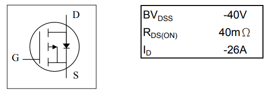
AP9563GH Overview
Representative AP9563GH image (package may vary by manufacturer)
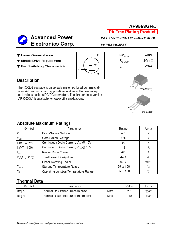
Description
The TO-252 package is universally preferred for all commercialindustrial surface mount applications and suited for low voltage applications such as DC/DC converters. The through-hole version (AP9563GJ) is available for low-profile applications.