AP9563GK
AP9563GK is P-CHANNEL ENHANCEMENT MODE POWER MOSFET manufactured by Advanced Power Electronics Corp.
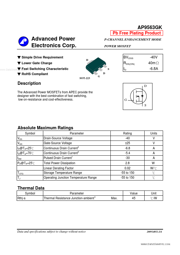
Description
The Advanced Power MOSFETs from APEC provide the designer with the best bination of fast switching, low on-resistance and cost-effectiveness.
Absolute Maximum Ratings
Symbol VDS VGS ID@TA=25℃ ID@TA=70℃ IDM PD@TA=25℃ TSTG TJ Parameter Drain-Source Voltage Gate-Source Voltage Continuous Drain Current Continuous Drain Current Pulsed Drain Current
1 3 3
Rating -40 ±25 -6.8 -5.4 -30 2.8 0.02 -55 to 150 -55 to 150
Units V V A A A W W/ ℃ ℃ ℃
Total Power Dissipation Linear Derating Factor Storage Temperature Range Operating Junction Temperature Range
Thermal Data
Symbol Rthj-a Parameter Thermal Resistance Junction-ambient
Value Max. 45
Unit ℃/W
Data and specifications subject to change without notice
200914051-1/4
Electrical Characteristics@Tj=25o C(unless otherwise specified)
Symbol BVDSS
ΔBVDSS/ΔTj
Parameter Drain-Source Breakdown Voltage
Test Conditions VGS=0V, ID=-250u A
Min. -40 -1
- Typ. -0.03 10 20 4 10 12 6 70 36 240 185 5.8
Max. Units 40 60 -3 -1 -25 ±100 30 8.7 V V/℃ mΩ mΩ V S u A u A n A n C n C n C ns ns ns ns p F p F p F Ω
Breakdown Voltage Temperature Coefficient Reference to 25℃, ID=-1m A
RDS(ON)
..
Static Drain-Source On-Resistance
VGS=-10V, ID=-6A VGS=-4.5V, ID=-4A
VGS(th) gfs IDSS IGSS Qg Qgs Qgd td(on) tr td(off) tf Ciss Coss Crss Rg
Gate Threshold Voltage Forward Transconductance
Drain-Source Leakage Current (Tj=25o C) Drain-Source Leakage Current (Tj=70 C) o
VDS=VGS, ID=-250u A VDS=-10V, ID=-6A VDS=-40V, VGS=0V VDS=-32V, VGS=0V VGS=±25V ID=-6A VDS=-32V VGS=-4.5V VDS=-20V ID=-1A RG=3.3Ω,VGS=-10V RD=20Ω VGS=0V VDS=-25V f=1.0MHz f=1.0MHz
Gate-Source Leakage Total Gate Charge
Gate-Source Charge Gate-Drain ("Miller") Charge Turn-on Delay Time Rise Time Turn-off Delay Time Fall Time Input Capacitance Output Capacitance Reverse Transfer Capacitance Gate Resistance
1600 2560
Source-Drain...