UT7R995C Key Features
- Total-dose tolerance: 100 krad (Si)
- SEL Immune to a LET of 109 MeV-cm2/mg
- SEU Immune to a LET of 109 MeV-cm2/mg Military temperature range: -55oC to +125oC Extended industrial temp: -40oC to +12
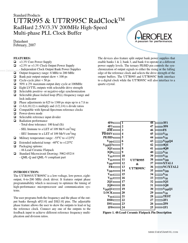
- 48-Lead Ceramic Flatpack Standard Microcircuit Drawing: 5962-05214
- QML-Q and QML-V pliant part