AS7C251MNTF32A
Description
Thermal resistance (junction to ambient)1 Thermal resistance (junction to top of case)1 1 This parameter is sampled Conditions 1-layer Test conditions follow standard test methods and procedures for measuring thermal impedance, per EIA/JESD51 4-layer Symbol θJA θJA θJC Typical 40 22 8 Units °C/W °C/W °C/W 12/23/04, v 1.1 Alliance Semiconductor P. 4 of 18 AS7C251MNTF32A/36A ® Signal descriptions Signal CLK CEN A, A0, A1 DQ[a,b,c,d] CE0, CE1, CE2 I/O Properties I I I I/O I I I I I I I CLOCK SYNC SYNC SYNC SYNC SYNC SYNC SYNC ASYNC STATIC ASYNC - Description Clock. All inputs except OE, LBO, and ZZ are synchronous to this clock.
Key Features
- Organization: 1,048,576 words × 32 or 36 bits NTD™architecture for efficient bus operation Fast clock to data access: 7.5/8.5/10 ns Fast OE access time: 3.5/4.0 ns Fully synchronous operation Flow-through mode Asynchronous output enable control Available in 100-pin TQFP package * * * * * *
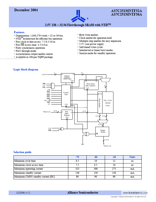
- Byte write enables Clock enable for operation hold Multiple chip enables for easy expansion 2.5V core power supply Self-timed write cycles Interleaved or linear burst modes Snooze mode for standby operation Logic block diagram A[19:0] 20
- Address register Burst logic Q 20