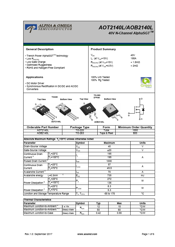
AOT2140L/AOB2140L
Electrical Characteristics (TJ=25°C unless otherwise noted)
Symbol Parameter
Conditions
STATIC PARAMETERS
BVDSS Drain-Source Breakdown Voltage
IDSS Zero Gate Voltage Drain Current
ID=250µA, VGS=0V
VDS=40V, VGS=0V
IGSS
VGS(th)
RDS(ON)
gFS
VSD
IS
Gate-Body leakage current
Gate Threshold Voltage
Static Drain-Source On-Resistance
VDS=0V, VGS=±20V
VDS=VGS, ID=250µA
VGS=10V, ID=20A
VGS=4.5V, ID=20A
Forward Transconductance
VDS=5V, ID=20A
Diode Forward Voltage
IS=1A, VGS=0V
Maximum Body-Diode Continuous Current G
TJ=55°C
TJ=125°C
DYNAMIC PARAMETERS
Ciss Input Capacitance
Coss Output Capacitance
Crss Reverse Transfer Capacitance
Rg Gate resistance
VGS=0V, VDS=20V, f=1MHz
f=1MHz
SWITCHING PARAMETERS
Qg(10V)
Qg(4.5V)
Qgs
Qgd
Qoss
tD(on)
tr
tD(off)
tf
trr
Qrr
Total Gate Charge
Total Gate Charge
Gate Source Charge
VGS=10V, VDS=20V, ID=20A
Gate Drain Charge
Output Charge
Turn-On DelayTime
VGS=0V, VDS=20V
Turn-On Rise Time
Turn-Off DelayTime
VGS=10V, VDS=20V, RL=1Ω,
RGEN=3Ω
Turn-Off Fall Time
Body Diode Reverse Recovery Time IF=20A, di/dt=500A/µs
Body Diode Reverse Recovery Charge IF=20A, di/dt=500A/µs
Min
40
1.3
1.3
Typ
1.8
1.2
1.75
1.5
100
0.66
9985
1635
95
2.6
128
54
29
11
67
16
16
125
27
29
107
Max Units
1
5
±100
2.3
1.5
2.2
2.0
1
195
V
µA
nA
V
mΩ
mΩ
S
V
A
pF
pF
pF
3.9 Ω
180 nC
80 nC
nC
nC
nC
ns
ns
ns
ns
ns
nC
A. The value of RθJA is measured with the device mounted on 1in2 FR-4 board with 2oz. Copper, in a still air environment with TA =25°C. The
Power dissipation PDSM is based on R θJA t≤ 10s and the maximum allowed junction temperature of 150°C. The value in any given application
depends on the user's specific board design, and the maximum temperature of 175°C may be used if the PCB allows it.
B. The power dissipation PD is based on TJ(MAX)=175°C, using junction-to-case thermal resistance, and is more useful in setting the upper
dissipation limit for cases where additional heatsinking is used.
C. Single pulse width limited by junction temperature TJ(MAX)=175°C.
D. The RθJA is the sum of the thermal impedance from junction to case RθJC and case to ambient.
E. The static characteristics in Figures 1 to 6 are obtained using <300µs pulses, duty cycle 0.5% max.
F. These curves are based on the junction-to-case thermal impedance which is measured with the device mounted to a large heatsink, assuming
a maximum junction temperature of TJ(MAX)=175°C. The SOA curve provides a single pulse rating.
G. The maximum current rating is package limited.
H. These tests are performed with the device mounted on 1 in2 FR-4 board with 2oz. Copper, in a still air environment with TA=25°C.
APPLICATIONS OR USE AS CRITICAL COMPONENTS IN LIFE SUPPORT DEVICES OR SYSTEMS ARE NOT AUTHORIZED. AOS DOES NOT
ASSUME ANY LIABILITY ARISING OUT OF SUCH APPLICATIONS OR USES OF ITS PRODUCTS. AOS RESERVES THE RIGHT TO IMPROVE
PRODUCT DESIGN,FUNCTIONS AND RELIABILITY WITHOUT NOTICE.
Rev.1.0: September 2017
www.aosmd.com
Page 2 of 6