Datasheet Details
| Part number | AOD421 |
|---|---|
| Manufacturer | Alpha & Omega Semiconductors |
| File Size | 144.02 KB |
| Description | P-Channel MOSFET |
| Datasheet |
 AOD421 Datasheet AOD421 Datasheet
|
|
|
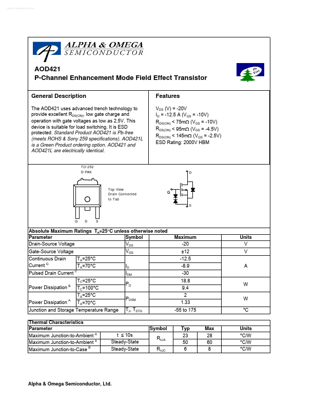
The AOD421 uses advanced trench technology to provide excellent RDS(ON), low gate charge and operation with gate voltages as low as 2.5V.
This device is suitable for load switching.
It is ESD protected.
| Part number | AOD421 |
|---|---|
| Manufacturer | Alpha & Omega Semiconductors |
| File Size | 144.02 KB |
| Description | P-Channel MOSFET |
| Datasheet |
AOD421 Datasheet
|
|
|
|
| Part Number | Description | Manufacturer |
|---|---|---|
| AOD421 | N-Channel MOSFET | INCHANGE |
| AOD422 | N-Channel MOSFET | INCHANGE |
| AOD423 | P-Channel MOSFET | INCHANGE |
| AOD424 | N-Channel MOSFET | INCHANGE |
| AOD424G | N-Channel MOSFET | INCHANGE |
| Part Number | Description |
|---|---|
| AOD420 | N-Channel MOSFET |
| AOD422 | N-Channel MOSFET |
| AOD423 | P-Channel MOSFET |
| AOD424 | 20V N-Channel MOSFET |
| AOD424G | N-Channel MOSFET |
The following content is an automatically extracted verbatim text from the original manufacturer datasheet and is provided for reference purposes only.