D452 Overview
Key Features
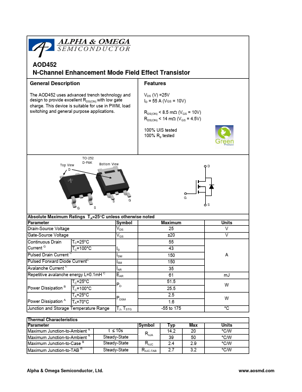
- The AOD452 uses advanced trench technology and design to provide excellent RDS(ON) with low gate charge
- This device is suitable for use in PWM, load switching and general purpose applications
| Part | D452 |
|---|---|
| Description | N-Channel MOSFET |
| Category | MOSFET |
| Manufacturer | Alpha & Omega Semiconductors |
| Size | 128.29 KB |
| Part Number | Manufacturer | Description |
|---|---|---|
| D452A | VBsemi | N-Channel MOSFET |
| D4556 | Sumc | Single-supply Dual High Current Operational |
| D4558 | DMS Microelectronic | Dual Operational Amplifier |
| D45C12 | Inchange Semiconductor | Silicon PNP Power Transistors |
| D4564841G5 | Unknown Manufacturer | UPD4564841G5 |