D5N50
Description
Product Summary
The AOD5N50 is fabricated using an advanced high voltage MOSFET process that is designed to deliver high levels of performance and robustness in popular AC-DC applications.By providing low RDS(on), Ciss and Crss along with guaranteed avalanche capability this device can be adopted quickly into new and existing offline power supply designs.
VDS ID (at VGS=10V) RDS(ON) (at VGS=10V)
100% UIS Tested! 100% Rg Tested!
600V@150℃
5A < 1.6Ω
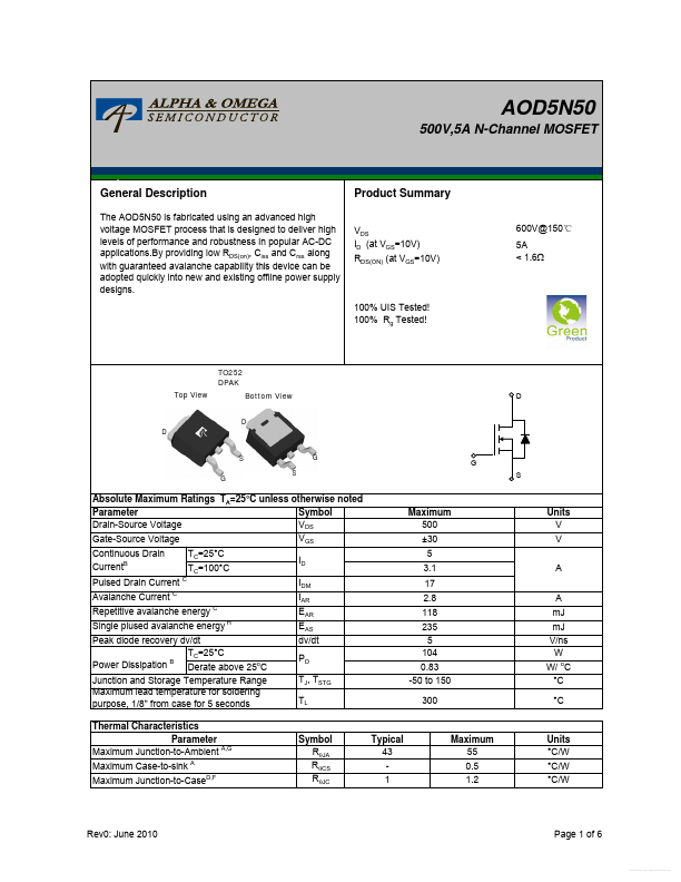
Top View
TO252 DPAK
Bottom View
Absolute Maximum Ratings TA=25°C unless otherwise noted
Parameter
Symbol
Drain-Source Voltage
Gate-Source Voltage
Continuous Drain
TC=25°C
Current B
TC=100°C
Pulsed Drain Current C
Avalanche Current C
Repetitive avalanche energy C
Single plused avalanche energy H
IDM IAR EAR EAS
Peak diode recovery dv/dt dv/dt
TC=25°C Power Dissipation B Derate above 25o C
Junction and Storage Temperature Range Maximum lead temperature for soldering purpose,...