Datasheet4U Logo Datasheet4U.com

AN10E40 - Field Programmable Analog Array

Datasheet Summary

Description

19 Package Pin Electrical Characterization 22 Powers, Grounds and Bypassing 22 Recommended Configuration for Power & Ground

Features

  • are directed by an on-chip SRAM configuration memory. The SRAM configuration memory is initialized on power up via an off chip serial PROM or through the AN10E40Õs standard microprocessor peripheral interface. A configuration memory image is easily constructed using the companion AnadigmDesigner¨ software which includes an extensive library of adjustable, proven, pre-built functions. The configurable analog blocks are often consumed one at a time, though some of the more complex library function.

📥 Download Datasheet

Datasheet preview – AN10E40

Datasheet Details

Part number AN10E40
Manufacturer Anadigm
File Size 354.07 KB
Description Field Programmable Analog Array
Datasheet download datasheet AN10E40 Datasheet
Additional preview pages of the AN10E40 datasheet.
Other Datasheets by Anadigm

Full PDF Text Transcription

Click to expand full text
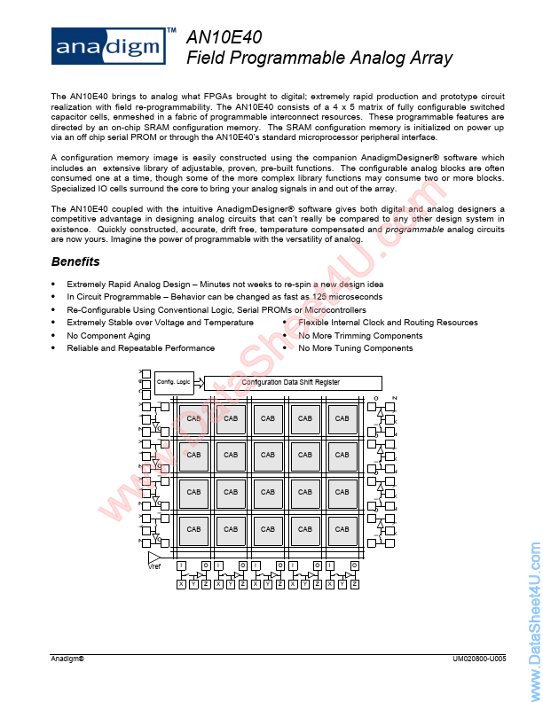
AN10E40 Field Programmable Analog Array The AN10E40 brings to analog what FPGAs brought to digital; extremely rapid production and prototype circuit realization with field re-programmability. The AN10E40 consists of a 4 x 5 matrix of fully configurable switched capacitor cells, enmeshed in a fabric of programmable interconnect resources. These programmable features are directed by an on-chip SRAM configuration memory. The SRAM configuration memory is initialized on power up via an off chip serial PROM or through the AN10E40Õs standard microprocessor peripheral interface. A configuration memory image is easily constructed using the companion AnadigmDesigner¨ software which includes an extensive library of adjustable, proven, pre-built functions.
Published: |