ADG1436
ADG1436 is Dual SPDT Switch manufactured by Analog Devices.
FEATURES
1.5 Ω on resistance 0.3 Ω on-resistance flatness 0.1 Ω on-resistance match between channels Continuous current per channel
LFCSP package: up to 400 m A TSSOP package: up to 260 m A Fully specified at +12 V, ±15 V, and ±5 V No VL supply required 3 V logic-patible inputs Rail-to-rail operation 16-lead TSSOP and 4 mm × 4 mm, 16-lead LFCSP packages
APPLICATIONS
Automatic test equipment Data acquisition systems Battery-powered systems Sample-and-hold systems Audio signal routing munication systems Relay replacement
FUNCTIONAL BLOCK DIAGRAMS
S1A D1
S1B
IN1
IN2
S2A D2
S2B
06817-001
SWITCHES SHOWN FOR A ONE-INPUT LOGIC.
Figure 1. TSSOP Package
S1A
S2A
D1
D2
S1B
S2B
LOGIC
GENERAL DESCRIPTION
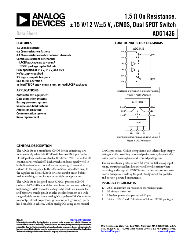
The ADG1436 is a monolithic CMOS device containing two independently selectable SPDT switches. An EN input on the LFCSP package enables or disable the device. When disabled, all channels are switched off. Each switch conducts equally well in both directions when on and has an input signal range that extends to the supplies. In the off condition, signal levels up to the supplies are blocked. Both switches exhibit break-beforemake switching action for use in multiplexer applications.
The ADG1436 is designed on an i CMOS® process. i CMOS (industrial-CMOS) is a modular manufacturing process bining high voltage CMOS (plementary metal-oxide semiconductor) and bipolar technologies. It enables the development of a wide range of high performance analog ICs capable of 33 V operation in a footprint that no previous generation of high voltage parts has been able to achieve. Unlike analog ICs using conventional
IN1 IN2 EN
SWITCHES SHOWN FOR A ONE-INPUT LOGIC.
Figure 2. LFCSP Package
CMOS processes, i CMOS ponents can tolerate high supply voltages while providing increased performance, dramatically lower power consumption, and reduced package size. The on-resistance profile is very flat over the full analog input range, ensuring excellent linearity and low distortion...