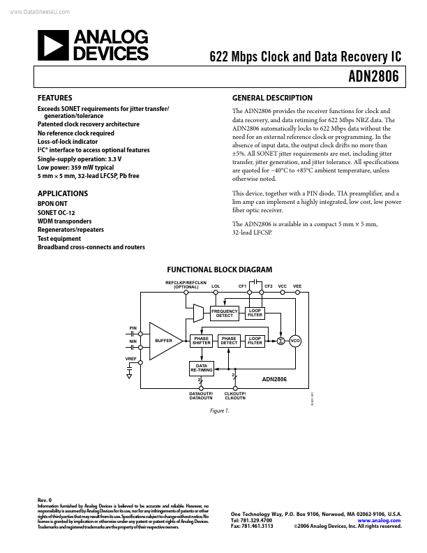
Datasheet4U Logo Datasheet4U.com

ADN2806 Datasheet - Analog Devices

Clock and Data Recovery IC

ADN2806 Features

* Exceeds SONET requirements for jitter transfer/ generation/tolerance Patented clock recovery architecture No reference clock required Loss-of-lock indicator I2C® interface to access optional features Single-supply operation: 3.3 V Low power: 359 mW typical 5 mm × 5 mm, 32-lead LFCSP, Pb free GENERA

ADN2806 General Description

The ADN2806 provides the receiver functions for clock and data recovery, and data retiming for 622 Mbps NRZ data. The ADN2806 automatically locks to 622 Mbps data without the need for an external reference clock or programming. In the absence of input data, the output clock drifts no more than ±5%. .

ADN2806 Datasheet (322.80 KB)

Preview of ADN2806 PDF

Datasheet Details

Part number:

ADN2806

Manufacturer:

Analog Devices ↗

File Size:

322.80 KB

Description:

Clock and data recovery ic.

📁 Related Datasheet

ADN2804 Clock and Data Recovery (Analog Devices)

ADN2805 1.25 Gbps Clock and Data Recovery IC (Analog Devices)

ADN2807 Clock and Data Recovery (Analog Devices)

ADN2809 Multi-Rate to 2.7Gbps Clock and Data Recovery IC with Limiting Amplifier (Analog Devices)

ADN2811 OC-48/OC-48 FEC Clock and Data Recovery IC (Analog Devices)

ADN2812 Continuous Rate 12.3 Mb/s to 2.7 Gb/s Clock and Data Recovery IC with Integrated Limiting Amp (Analog Devices)

ADN2813 Clock and Data Recovery IC (Analog Devices)

ADN2814 Continuous Rate 10 Mb/s to 675 Mb/s Clock and Data Recovery (Analog Devices)

ADN2815 Clock and Data Recovery IC (Analog Devices)

ADN2816 Continuous Rate 12.3 Mb/s to 675 Mb/s Clock and Data Recovery IC (Analog Devices)

TAGS

ADN2806 Clock and Data Recovery Analog Devices

Image Gallery

ADN2806 Datasheet Preview Page 2 ADN2806 Datasheet Preview Page 3

ADN2806 Distributor