ADN2807
ADN2807 is Clock and Data Recovery manufactured by Analog Devices.
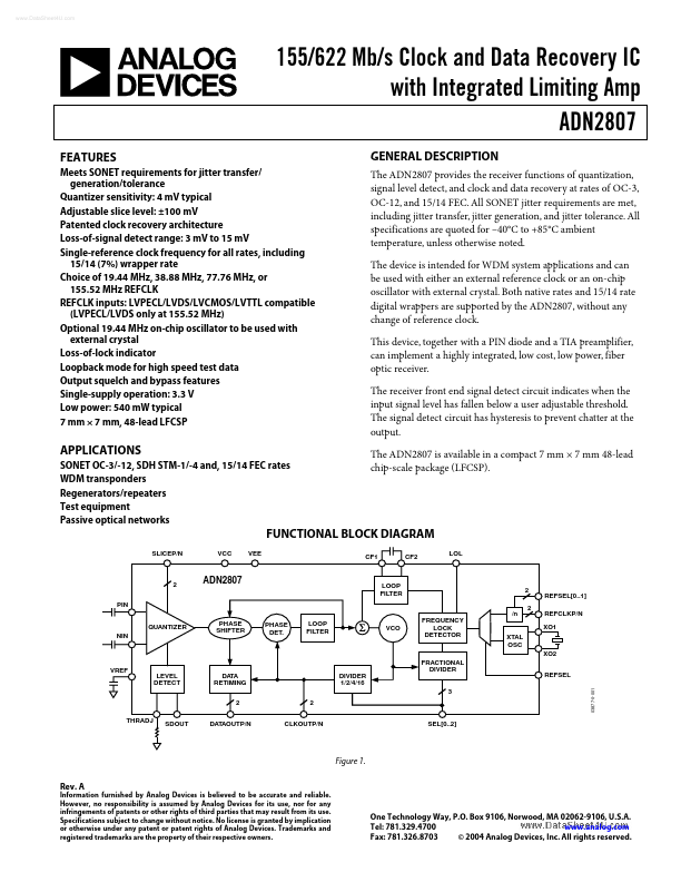
..
155/622 Mb/s Clock and Data Recovery IC with Integrated Limiting Amp ADN2807
Features
Meets SONET requirements for jitter transfer/ generation/tolerance Quantizer sensitivity: 4 mV typical Adjustable slice level: ±100 mV Patented clock recovery architecture Loss-of-signal detect range: 3 mV to 15 mV Single-reference clock frequency for all rates, including 15/14 (7%) wrapper rate Choice of 19.44 MHz, 38.88 MHz, 77.76 MHz, or 155.52 MHz REFCLK REFCLK inputs: LVPECL/LVDS/LVCMOS/LVTTL patible (LVPECL/LVDS only at 155.52 MHz) Optional 19.44 MHz on-chip oscillator to be used with external crystal Loss-of-lock indicator Loopback mode for high speed test data Output...