Datasheet4U Logo Datasheet4U.com

ADN2892 Datasheet - Analog Devices

Limiting Amplifier

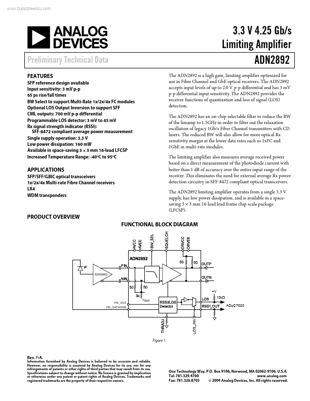
ADN2892 Features

* SFP reference design available Input sensitivity: 3 mV p-p 65 ps rise/fall times BW Select to support Multi-Rate 1x/2x/4x FC modules Optional LOS Output Inversion to support SFF CML outputs: 700 mV p-p differential Programmable LOS detector: 3 mV to 45 mV Rx signal strength indicator (RSSI): SFF-847

ADN2892 General Description

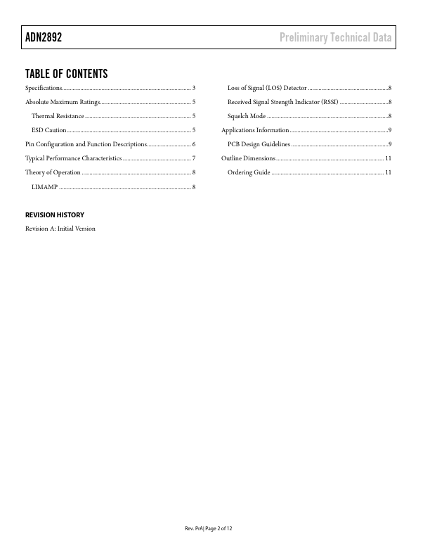
6 Typical Performance Characteristics 7 Theory of Operation 8 LIMAMP 8 Preliminary Technical Data Loss of Signal (LOS) Detector 8 Received Signal Strength Indicator (RSSI) 8 Squelch Mode 8 Applications Information 9 PCB Design Guidelines 9 Outline Dimensions 11 Ordering Guide 11 REVISION HI.

ADN2892 Datasheet (259.97 KB)

Preview of ADN2892 PDF

Datasheet Details

Part number:

ADN2892

Manufacturer:

Analog Devices ↗

File Size:

259.97 KB

Description:

Limiting amplifier.

📁 Related Datasheet

ADN2890 Limiting Amplifier (Analog Devices)

ADN2891 Amplifier (Analog Devices)

ADN2804 Clock and Data Recovery (Analog Devices)

ADN2805 1.25 Gbps Clock and Data Recovery IC (Analog Devices)

ADN2806 Clock and Data Recovery IC (Analog Devices)

ADN2807 Clock and Data Recovery (Analog Devices)

ADN2809 Multi-Rate to 2.7Gbps Clock and Data Recovery IC with Limiting Amplifier (Analog Devices)

ADN2811 OC-48/OC-48 FEC Clock and Data Recovery IC (Analog Devices)

ADN2812 Continuous Rate 12.3 Mb/s to 2.7 Gb/s Clock and Data Recovery IC with Integrated Limiting Amp (Analog Devices)

ADN2813 Clock and Data Recovery IC (Analog Devices)

TAGS

ADN2892 Limiting Amplifier Analog Devices

Image Gallery

ADN2892 Datasheet Preview Page 2 ADN2892 Datasheet Preview Page 3

ADN2892 Distributor