Datasheet4U Logo Datasheet4U.com

ADN4694E - (ADN4690E - ADN4695E) High Speed M-LVDS Transceivers

General Description

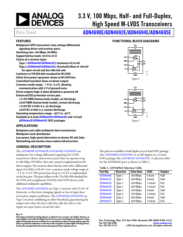
The ADN4690E/ADN4692E/ADN4694E/ADN4695E are multipoint, low voltage differential signaling (M-LVDS) transceivers (driver and receiver pairs) that can operate at up to 100 Mbps (50 MHz).

Slew rate control is implemented on the driver outputs.

Key Features

  • Multipoint LVDS transceivers (low voltage differential signaling driver and receiver pairs) Switching rate: 100 Mbps (50 MHz) Supported bus loads: 30 Ω to 55 Ω Choice of 2 receiver types Type 1 (ADN4690E/ADN4692E): hysteresis of 25 mV Type 2 (ADN4694E/ADN4695E): threshold offset of 100 mV for open-circuit and bus-idle fail-safe Conforms to TIA/EIA-899 standard for M-LVDS Glitch-free power-up/power-down on M-LVDS bus Controlled transition times on driver output Common-mode range:.
  • 1 V to.

📥 Download Datasheet

Datasheet Details

Part number ADN4694E
Manufacturer Analog Devices
File Size 760.69 KB
Description (ADN4690E - ADN4695E) High Speed M-LVDS Transceivers
Datasheet download datasheet ADN4694E Datasheet

Full PDF Text Transcription (Reference)

The following content is an automatically extracted verbatim text from the original manufacturer datasheet and is provided for reference purposes only.

View original datasheet text
3.3 V, 100 Mbps, Half- and Full-Duplex, High Speed M-LVDS Transceivers Data Sheet FEATURES Multipoint LVDS transceivers (low voltage differential signaling driver and receiver pairs) Switching rate: 100 Mbps (50 MHz) Supported bus loads: 30 Ω to 55 Ω Choice of 2 receiver types Type 1 (ADN4690E/ADN4692E): hysteresis of 25 mV Type 2 (ADN4694E/ADN4695E): threshold offset of 100 mV for open-circuit and bus-idle fail-safe Conforms to TIA/EIA-899 standard for M-LVDS Glitch-free power-up/power-down on M-LVDS bus Controlled transition times on driver output Common-mode range: −1 V to +3.