Datasheet4U Logo Datasheet4U.com

ADP1196 Datasheet - Analog Devices

High-Side or Low-Side Load Switch

ADP1196 Features

* Low RDSON of 10 mΩ in 6-ball WLCSP Wide input voltage range: 0 V to 5.5 V 3 A continuous operating current at 70°C Bias supply voltage range: 1.83 V to 5.5 V Low 26 µA ground (quiescent) current, VIN ≤ 3.4 V Low 50 µA quiescent current, VIN = 5.5 V Overtemperature protection circuitry Low shutdown c

ADP1196 General Description

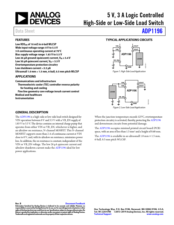
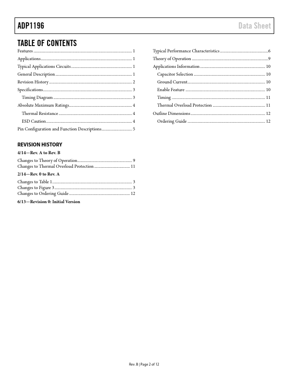
The ADP1196 is a high-side or low-side load switch designed for VIN operation between 0 V and 5.5 V with a VB_EN supply of 1.83 V to 5.5 V. The device contains an internal charge pump that operates from either VIN or VB_EN, whichever is higher, and an ultralow on resistance, N-channel MOSFET. This N.

ADP1196 Datasheet (368.25 KB)

Preview of ADP1196 PDF

Datasheet Details

Part number:

ADP1196

Manufacturer:

Analog Devices ↗

File Size:

368.25 KB

Description:

High-side or low-side load switch.

📁 Related Datasheet

ADP1190 Integrated 500 mA Load Switch (Analog Devices)

ADP1190A Integrated 500 mA Load Switch (Analog Devices)

ADP1191 PRECISION SEMICONDUCTOR PRESSURE SENSOR (ETC)

ADP1101 PRECISION SEMICONDUCTOR PRESSURE SENSOR (ETC)

ADP1108 DC-to-DC Converter (Analog Devices)

ADP1109 DC-to-DC Converter (Analog Devices)

ADP1109A DC-to-DC Converter (Analog Devices)

ADP1110 Step-Up/Step-Down Switching Regulator (Analog Devices)

ADP1111 Step-Up/Step-Down SW Regulator (Analog Devices)

ADP1111 PRECISION SEMICONDUCTOR PRESSURE SENSOR (ETC)

TAGS

ADP1196 High-Side Low-Side Load Switch Analog Devices

Image Gallery

ADP1196 Datasheet Preview Page 2 ADP1196 Datasheet Preview Page 3

ADP1196 Distributor