ADPA1113
ADPA1113 is GaN Power Amplifier manufactured by Analog Devices.
FEATURES
- Internally matched and AC-coupled, 40 W, Ga N power amplifier
- Integrated drain bias inductor
- POUT: 46.5 d Bm typical from 2.0 GHz to 5.7 GHz (PIN = 21 d Bm)
- Small signal gain: 40.5 d B typical from 2.3 GHz to 5.7 GHz
- Power gain: 25.5 d B typical from 2.0 GHz to 5.7 GHz (PIN = 21 d Bm)
- PAE: 39% typical from 2.3 GHz to 5.7 GHz
- VDD = 28 V at IDQ = 750 m A
- 14-lead ceramic leaded chip carrier [LDCC] with a copper-molyb- denum base
APPLICATIONS
- Military jammers
- mercial and military radars
- Test and measurement equipment
GENERAL DESCRIPTION
The ADPA1113 is a gallium nitride (Ga N), broadband power amplifier delivering 46.5 d Bm (44.7 W) with 39.0% power added efficiency (PAE) from 2.3 GHz to 5.7 GHz. No external matching or AC-coupling are required to achieve full-band operation. Additionally, no external inductor is required to bias the amplifier.
The ADPA1113 is ideal for continuous wave applications, such as military jammers and radars.
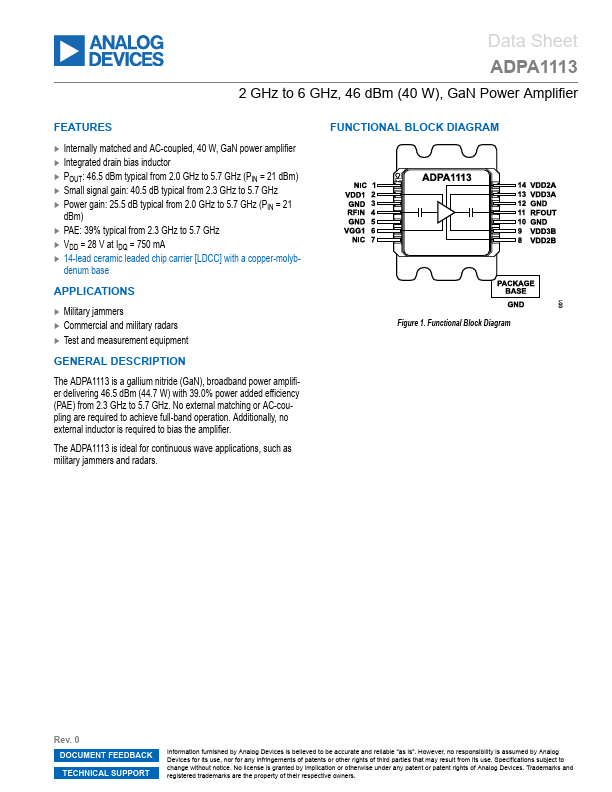
FUNCTIONAL BLOCK DIAGRAM
Figure 1. Functional Block Diagram
Rev. 0 DOCUMENT FEEDBACK TECHNICAL SUPPORT
Information furnished by Analog Devices is believed to be accurate and reliable "as is". However, no responsibility is assumed by Analog Devices for its use, nor for any infringements of patents or other rights of third parties that may result from its use. Specifications subject to change without notice. No license is granted by implication or otherwise under any patent or patent rights of Analog Devices. Trademarks and registered trademarks are the property of their respective owners.
Data Sheet
TABLE OF CONTENTS
Features
1 Applications 1 General Description
1 Functional Block Diagram 1 Specifications 3
Electrical Specifications...