Datasheet4U Logo Datasheet4U.com

ADPA1116 - GaN Power Amplifier

General Description

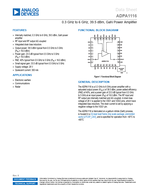
The ADPA1116 is a 0.3 GHz to 6 GHz power amplifier with a saturated output power (POUT) of 39.5 dBm, power added efficiency (PAE) of 40%, and a power gain of 23.5 dB typical from 0.5 GHz to 5 GHz at an input power (PIN) of 16.0 dBm.

The RF input and RF output are internally matched and AC-coupled.

Key Features

  • Internally matched, 0.3 GHz to 6 GHz, 39.5 dBm, GaN power amplifier.
  • RF input and RF output AC-coupled.
  • Integrated drain bias inductors.
  • Output power: 39.5 dBm typical from 0.5 GHz to 5 GHz (PIN = 16.0 dBm).
  • Power gain: 23.5 dB typical from 0.5 GHz to 5 GHz (PIN = 16.0 dBm).
  • PAE: 40% typical from 0.5 GHz to 5 GHz (PIN = 16.0 dBm).
  • Small signal gain: 33.5 dB typical from 0.5 GHz to 5 GHz.
  • Supply voltage: 28 V.
  • Quiescent current: 300 mA.

📥 Download Datasheet

Full PDF Text Transcription (Reference)

The following content is an automatically extracted verbatim text from the original manufacturer datasheet and is provided for reference purposes only.

View original datasheet text
Data Sheet ADPA1116 0.3 GHz to 6 GHz, 39.5 dBm, GaN Power Amplifier FEATURES ► Internally matched, 0.3 GHz to 6 GHz, 39.5 dBm, GaN power amplifier ► RF input and RF output AC-coupled ► Integrated drain bias inductors ► Output power: 39.5 dBm typical from 0.5 GHz to 5 GHz (PIN = 16.0 dBm) ► Power gain: 23.5 dB typical from 0.5 GHz to 5 GHz (PIN = 16.0 dBm) ► PAE: 40% typical from 0.5 GHz to 5 GHz (PIN = 16.0 dBm) ► Small signal gain: 33.5 dB typical from 0.5 GHz to 5 GHz ► Supply voltage: 28 V ► Quiescent current: 300 mA APPLICATIONS ► Electronic warfare ► Communications ► Radar FUNCTIONAL BLOCK DIAGRAM Figure 1. Functional Block Diagram GENERAL DESCRIPTION The ADPA1116 is a 0.3 GHz to 6 GHz power amplifier with a saturated output power (POUT) of 39.