Datasheet Summary
SHARC Processor ADSP-21367/ADSP-21368/ADSP-21369
SUMMARY
High performance 32-bit/40-bit floating-point processor optimized for high performance audio processing
Single-instruction, multiple-data (SIMD) putational architecture
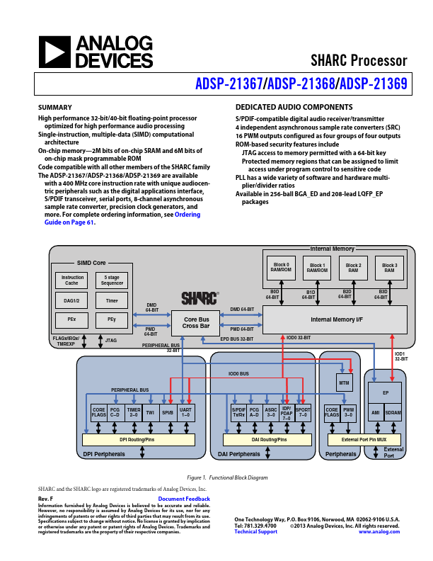
On-chip memory- 2M bits of on-chip SRAM and 6M bits of on-chip mask programmable ROM
Code patible with all other members of the SHARC family The ADSP-21367/ADSP-21368/ADSP-21369 are available with a 400 MHz core instruction rate with unique audiocentric peripherals such as the digital applications interface, S/PDIF transceiver, serial ports, 8-channel asynchronous sample rate converter, precision clock generators, and more. For plete ordering information, see...