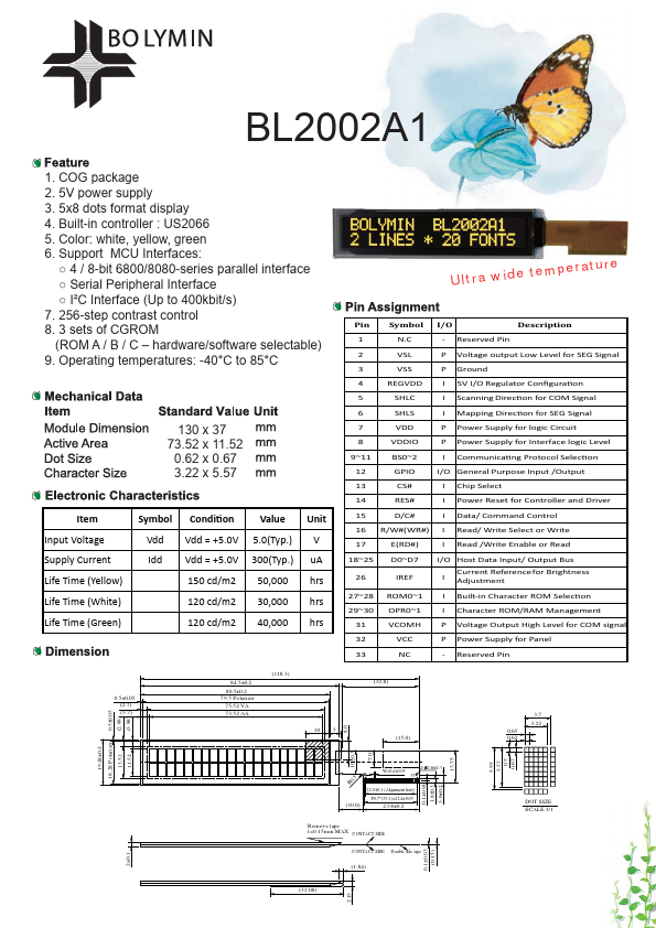
BL2002A1
BL2002A1 is DISPLAY manufactured by Bolymin.
Description
N.C
- Reserved Pin
P Voltage output Low Level for SEG Signal
P Ground
REGVDD
I 5V I/O Regulator ConfiguraƟon
SHLC
I Scanning DirecƟon for Signal
SHLS
I Mapping DirecƟon for SEG Signal
P Power Supply for logic Circuit
VDDIO
P Power Supply for Interface logic Level
9~11
BS0~2
I municaƟng Protocol SelecƟon
GPIO
I/O General Purpose Input /Output
13 CS# I Chip Select
14 RES# I Power Reset for Controller and Driver
15 D/C# I Data/ mand Control
16 R/W#(WR#) I Read/ Write Select or Write
E(RD#)
I Read /Write Enable or Read
18~25 26
D0~D7 IREF
I/O Host Data Input/ Output Bus Current Reference for Brightness
I Adjustment
27~28...