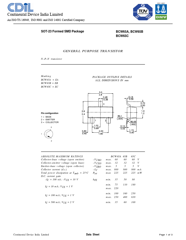
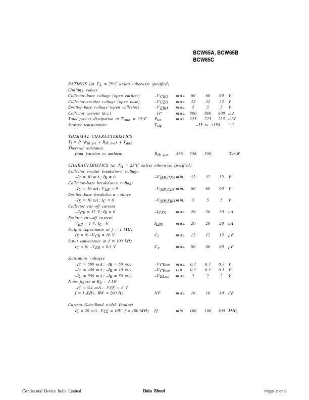
BCW65A Description
current gain IC = 100 mA; VCE = 2 V VCBO VCEO VEBO IC Ptot hFE BCW65A 65B max.
| Part number | BCW65A |
|---|---|
| Download | BCW65A Datasheet (PDF) |
| File Size | 78.57 KB |
| Manufacturer | Continental Device India |
| Description | GENERAL PURPOSE TRANSISTOR |
|
|
| Manufacturer | Part Number | Description |
|---|---|---|
| BCW65A | NPN Silicon AF Transistors | |
| BCW65A | NPN Silicon AF Transistor | |
| BCW65A | Surface mount Si-Epitaxial PlanarTransistors | |
| BCW65A | SILICON NPN TRANSISTORS | |
| BCW65A | GENERAL PURPOSE TRANSISTOR |
current gain IC = 100 mA; VCE = 2 V VCBO VCEO VEBO IC Ptot hFE BCW65A 65B max.