Click to expand full text
Continental Device India Limited
An ISO/TS 16949, ISO 9001 and ISO 14001 Certified Company
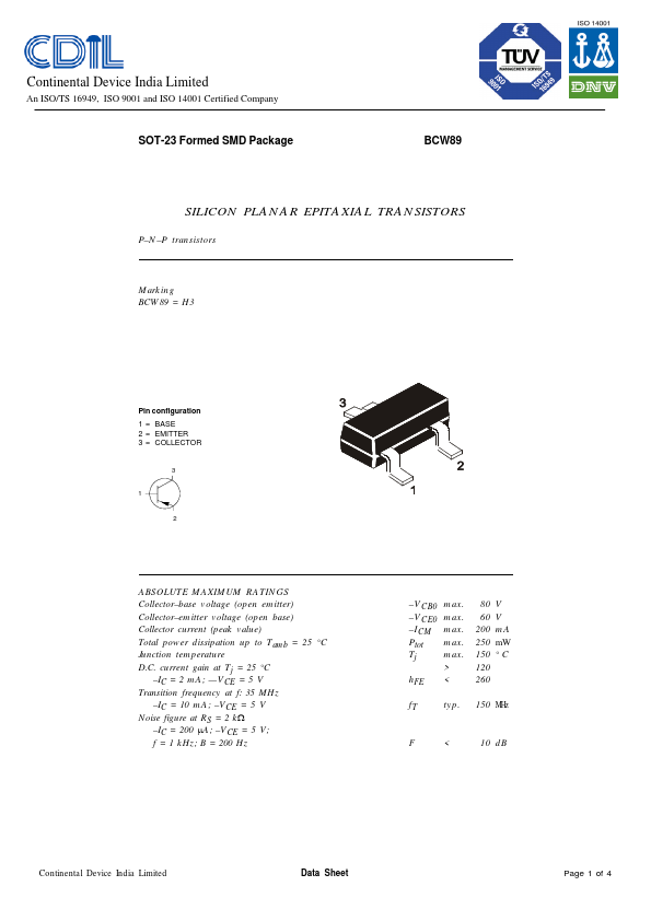
SOT-23 Formed SMD Package
BCW89
SILICON PLANAR EPITAXIAL TRANSISTORS
P–N–P transistors
Marking BCW89 = H3
Pin configuration 1 = BASE 2 = EMITTER 3 = COLLECTOR
3
1
2
ABSOLUTE MAXIMUM RATINGS Collector–base voltage (open emitter) Collector–emitter voltage (open base) Collector current (peak value) Total power dissipation up to Tamb = 25 °C Junction temperature D.C. current gain at Tj = 25 °C
–IC = 2 mA; —VCE = 5 V Transition frequency at f: 35 MHz
–IC = 10 mA; –VCE = 5 V Noise figure at RS = 2 kW
–IC = 200 mA; –VCE = 5 V; f = 1 kHz; B = 200 Hz
–VCB0 max. –VCE0 max. –ICM max. Ptot max. Tj max.
> hFE <
80 V 60 V 200 mA 250 mW 150 ° C 120 260
fT typ.