NXP Semiconductors BCW89
This data sheet contains target or goal specifications for product development. This data sheet contains preliminary data; supplementary data may be published later.| Part No. | BCW89 |
|---|---|
| Datasheet | BCW89 Download |
| Manufacturer |  NXP Semiconductors |
| Description | PNP general purpose transistor |
| Buy | Stock & Price |
FEATURES
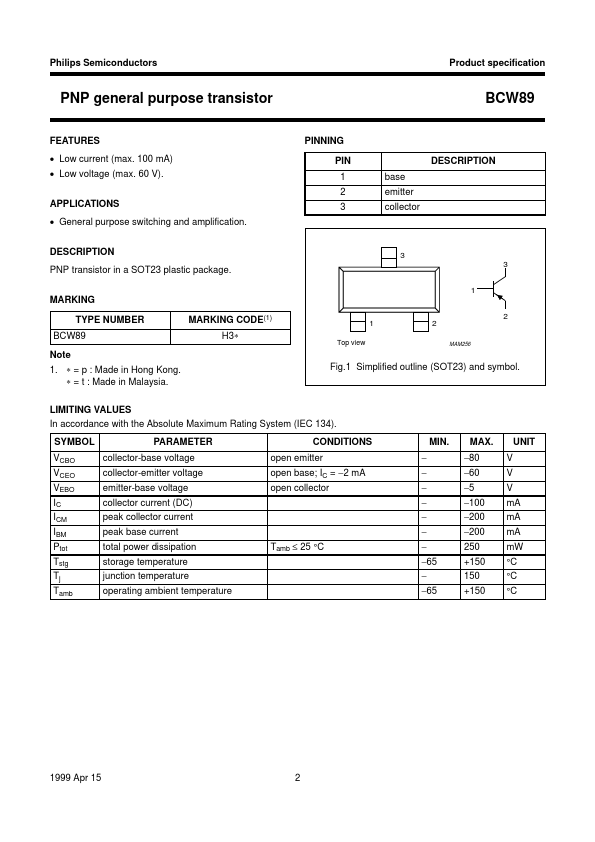
● Low current (max. 100 mA)● Low voltage (max. 60 V).
APPLICATIONS
● General purpose switching and amplification.DESCRIPTION
PNP transistor in a SOT23 plastic package. 1 handbook, halfpage BCW89 PINNING PIN 1 2 3 base emitter collectorDESCRIPTION
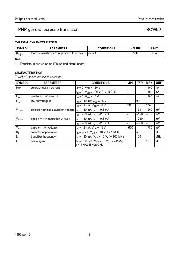
3 3 MARKING TYPE NUMBER BCW89 Note 1. ∗ = p : Made in Hong Kong. ∗ = t : Made in Malaysia. Fig.1 Simplified outline (SOT23) and symbol. MARKING CODE(1) H3∗ Top view 2 1 2 MAM256 LIMITING VALUES In accordance with the Absolute Maximum Rating System (IEC 134). SYMBOL VCBO VCEO VEBO IC ICM IBM Ptot Tstg Tj Tamb PARAMETER collector-base voltage collector-emitter voltage emitter-base voltage collector current (DC) peak collector current peak base current total power dissipation storage temperature junction temperature operating ambient temperature Tamb ≤ 25 °C CONDITIONS open emitter open base; IC = −2 mA open collector − − − − − − − −65 − −65 MIN. MAX. −80 −60 −5 −100 −200 −200 250 +150 150 +150 V V V mA mA mA mW °C °C °C UNIT 1999 Apr 15 2 Philips Semiconductors Product specification PNP general purpose transistor THERMAL CHARACTERISTICS SYMBOL Rth j-a Note 1.