CSD16414Q5 Description
N-Channel CICLON NexFET™ Power MOSFETs CSD16414Q5.
CSD16414Q5 Key Features
- Ultra Low Qg & Qgd
- Low Thermal Resistance
- Avalanche Rated
- Pb Free Terminal Plating
- RoHS pliant
- Halogen Free
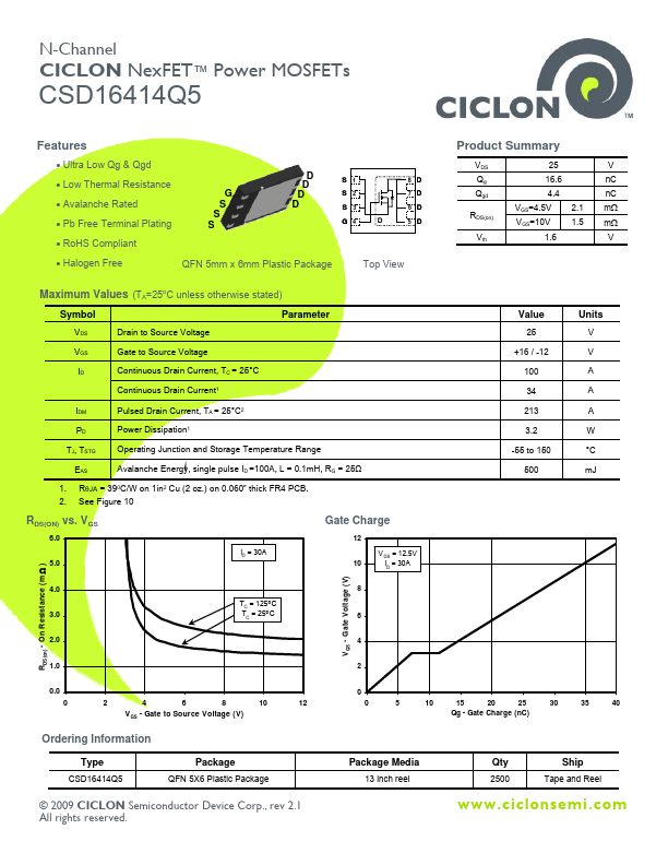
- On Resistance (m ) V GS
- Gate Voltage (V)
- Gate to Source Voltage (V)
- Gate Charge (nC)