MBR1060CT Overview
Key Specifications
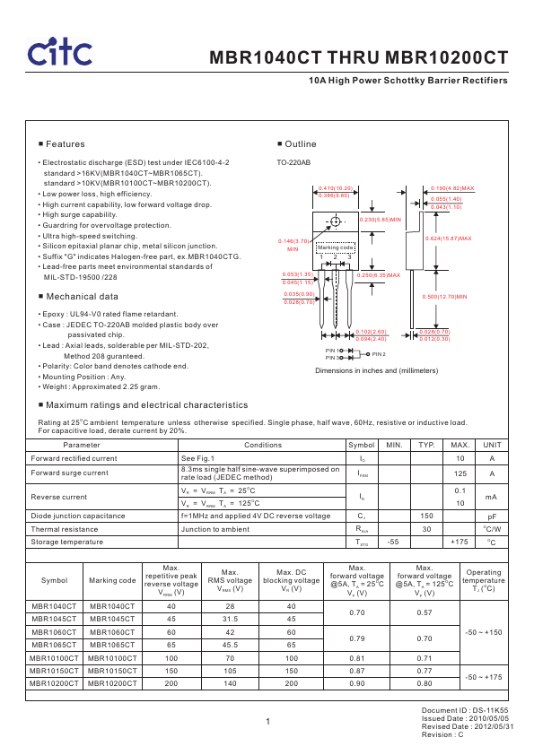
Package: TO-220-3
Mount Type: Through Hole
Max Operating Temp: 125 °C
Min Operating Temp: -55 °C
Key Features
- Low power loss, high efficiency
- High current capability, low forward voltage drop
- High surge capability
- Guardring for overvoltage protection
- Ultra high-speed switching
- Silicon epitaxial planar chip, metal silicon junction
- Suffix "G" indicates Halogen-free part, 1040CTG
- Lead-free parts meet environmental standards of MIL-STD-19500 /228
- Mechanical data
- Epoxy : UL94-V0 rated flame retardant