C450UT170 Overview
Key Specifications
Max Operating Temp: 100 °C
Min Operating Temp: -40 °C
Key Features
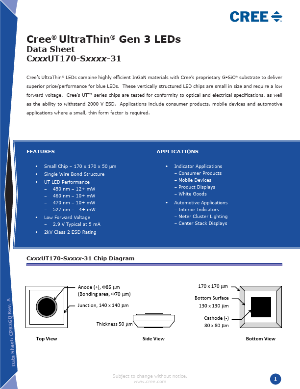
- Small Chip – 170 x 170 x 50 μm
- Single Wire Bond Structure
- UT LED Performance – 450 nm – 12+ mW – 460 nm – 10+ mW – 470 nm – 10+ mW – 527 nm – 4+ mW
- Low Forward Voltage – 2.9 V Typical at 5 mA
- 2kV Class 2 ESD Rating