MTA340N02KC3 Overview
Key Features
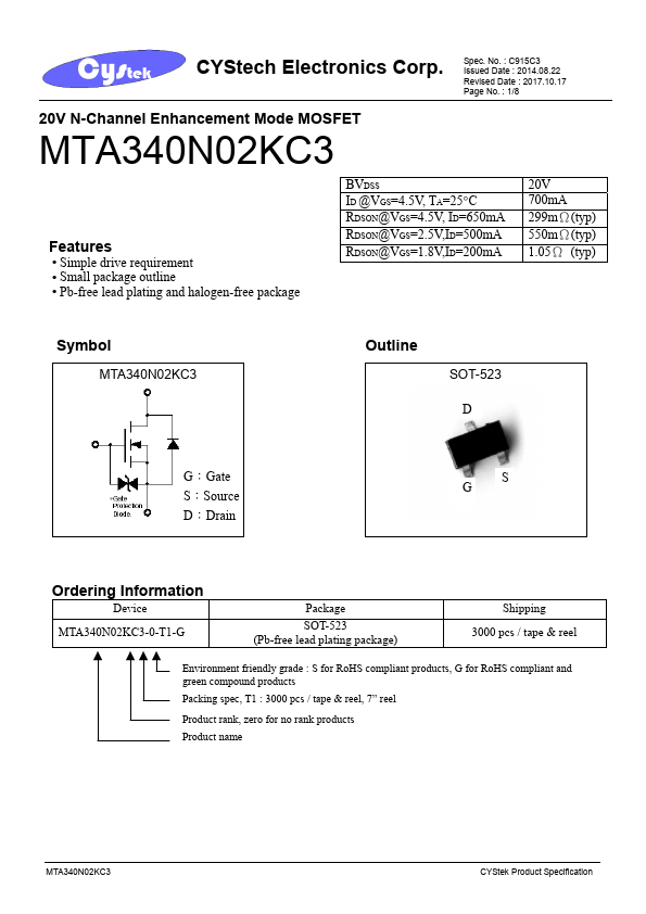
- Simple drive requirement
- Small package outline
| Part | MTA340N02KC3 |
|---|---|
| Description | N-Channel Enhancement Mode Power MOSFET |
| Category | MOSFET |
| Manufacturer | CYStech |
| Size | 403.38 KB |
| Part Number | Manufacturer | Description |
|---|---|---|
| A2SHB | HAOHAI | N-Channel MOSFET |
| AP9563GH | Advanced Power Electronics Corp | P-CHANNEL ENHANCEMENT MODE POWER MOSFET |
| FCPF360N65S3R0L | onsemi | N-Channel MOSFET |