
MTD5D0P03J3 Description
CYStech Electronics Corp. P-Channel Enhancement Mode Power MOSFET MTD5D0P03J3 Spec. 2018.04.13 Revised Date.
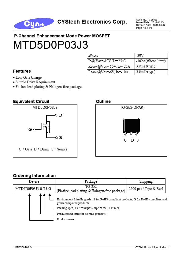
MTD5D0P03J3 Key Features
- Low Gate Charge
- Simple Drive Requirement
- Pb-free lead plating & Halogen-free package
- 30V -102A(silicon limit) 3.9mΩ(typ.) 5.6mΩ(typ.)