MTD5D0C03J4
MTD5D0C03J4 is N- & P-Channel Logic Level Enhancement Mode Power MOSFET manufactured by CYStech.
CYStech Electronics Corp.
Spec. No. : C704J4 Issued Date : 2017.08.28 Revised Date : 2017.12.06 Page No. : 1/13
N & P-Channel Enhancement Mode Power MOSFET
MTD5D0C03J4 BVDSS
ID @ VGS=10V(-10V), TA=25°C
ID @ VGS=10V(-10V), TC=25°C
Features
RDSON(typ.) @VGS=(-)10V
- Low Gate Charge
RDSON(typ.) @VGS=+4.5V(-5V)
- Simple Drive Requirement
- Ro HS pliant & Halogen-free package
N-CH 30V 8.6A
33.5A
7.7 mΩ
9.6 mΩ
P-CH -30V -6.0A
-23.0A
17.7mΩ
27.1 mΩ
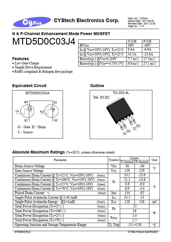
Equivalent Circuit
Outline
TO-252-4L Tab D1/D2
G:Gate D:Drain S:Source
S1G1...