J175 Overview
Key Features
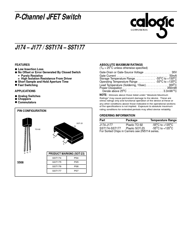
- J177 / SST174
- Low Insertion Loss
| Part | J175 |
|---|---|
| Description | P-Channel JFET Switch |
| Manufacturer | Calogic LLC |
| Size | 23.88 KB |
| Part Number | Manufacturer | Description |
|---|---|---|
| J175 | InterFET | P-Channel JFET |
| J175 | Fairchild Semiconductor | P-Channel Switch |
| J175 | NXP Semiconductors | P-channel silicon field-effect transistors |
| J175 | Vishay | P-Channel JFETs |
| J175 | onsemi | P-Channel Switch |