J175
Description
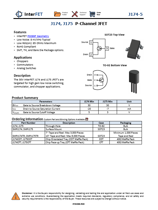
The 30V InterFET J174 and J175 JFET’s are targeted for high gain low noise switching, commutator, and chopper applications. Source 1 Drain 2 SOT23 Top View 3 Gate TO-92 Bottom View Drain 3 Gate 2 Source 1 Product Summary Parameters BVGSS Gate to Source Breakdown Voltage IDSS Drain to Source Saturation Current VGS(off) Gate to Source Cutoff Voltage J174 Min J175 Min Unit 30 30 V -20 -7 mA 5 3 V.
Key Features
- InterFET P0099F Geometry
- Low Noise: 8 nV/√Hz Typical
- Low Rds(on): 85 Ohms Maximum
- RoHS Compliant
- SMT, TH, and Bare Die Package options.