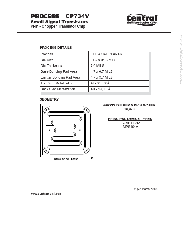
CP734V Description
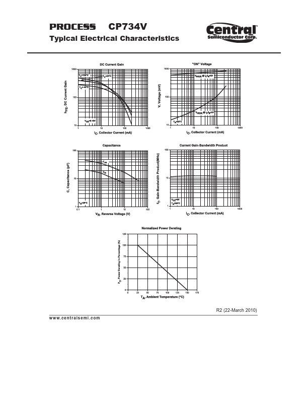
c o m R2 (22-March 2010) PROCESS CP734V Typical w w.
CP734V Key Features
- s e m i . c o m R2 (22-March 2010) PROCESS CP734V Typical
CP734V is NPN Transistor manufactured by Central Semiconductor.
| Part Number | Description |
|---|---|
| CP734V | PNP Transistor |
| CP704 | PNP Transistor |
| CP705 | PNP Transistor |
| CP707 | PNP Transistor |
| CP709 | PNP Transistor |
c o m R2 (22-March 2010) PROCESS CP734V Typical w w.