CP757X Description
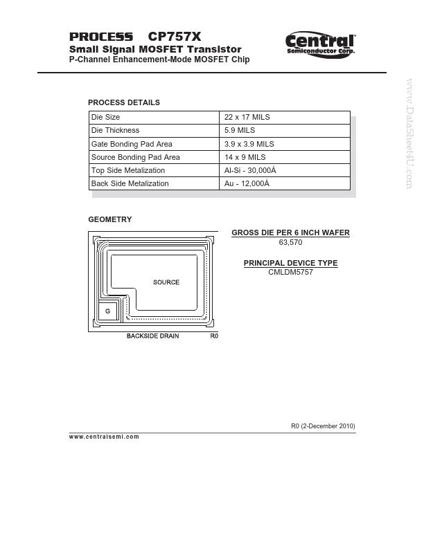
PROCESS Small Signal MOSFET Transistor P-Channel Enhancement-Mode MOSFET Chip CP757X .. c o m PROCESS CP757X Typical R0 (2-December 2010) w w.
CP757X Key Features
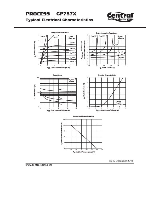
- s e m i . c o m PROCESS CP757X Typical
CP757X is P-Channel MOSFET manufactured by Central Semiconductor.
| Manufacturer | Part Number | Description |
|---|---|---|
| CP757 | PNP SILICON PLANAR EPITAXIAL TRANSISTORS |
PROCESS Small Signal MOSFET Transistor P-Channel Enhancement-Mode MOSFET Chip CP757X .. c o m PROCESS CP757X Typical R0 (2-December 2010) w w.