S27KS0642 Overview
S27KL0642/S27KS0642 3.0 V/1.8 V, 64 Mb (8 MB), HyperRAM Self-Refresh DRAM S27KL0642/S27KS0642, 3.0 V/1.8 V, 64 Mb (8 MB), HyperRAM Self-Refresh.
S27KS0642 Key Features
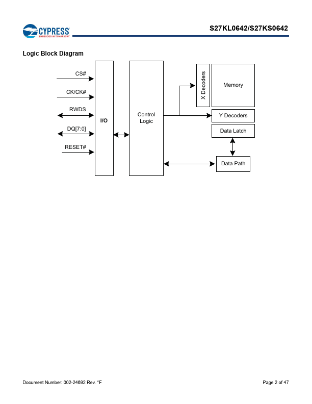
- HyperBus Interface
- 1.8 V / 3.0 V interface support
- Single-ended clock (CK)
- 11 bus signals
- Optional differential clock (CK, CK#)
- 12 bus signals
- Chip Select (CS#)
- 8-bit data bus (DQ[7:0])
- Hardware reset (RESET#)
- Bidirectional Read-Write Data Strobe (RWDS)