CY2DP1504
Overview
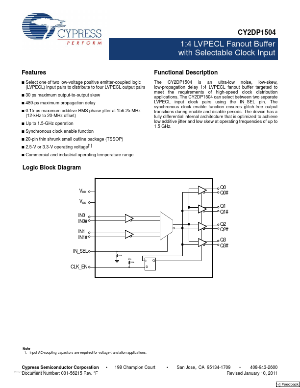
- Functional Description The CY2DP1504 is an ultra-low noise, low-skew, low-propagation delay 1:4 LVPECL fanout buffer targeted to meet the requirements of high-speed clock distribution applications. The CY2DP1504 can select between two separate LVPECL input clock pairs using the IN_SEL pin. The synchronous clock enable function ensures glitch-free output transitions during enable and disable periods. The device has a fully differential internal architecture that is optimized to achieve low additive jitter and low skew at operating frequencies of up to 1.5 GHz. Select one of two low-voltage positive emitter-coupled logic (LVPECL) input pairs to distribute to four LVPECL output pairs 30 ps maximum output-to-output skew 480-ps maximum propagation delay 0.15-ps maximum additive RMS phase jitter at 156.25 MHz (12-kHz to 20-MHz offset) Up to 1.5-GHz operation Synchronous clock enable function 20-pin thin shrunk small outline package (TSSOP) 2.5-V or 3.3-V operating voltage[1] Commercial and industrial operating temperature range Logic Block Diagram