CY2DP1502
CY2DP1502 is 1:2 LVPECL Fanout Buffer manufactured by Cypress.
1:2 LVPECL Fanout Buffer
1:2 LVPECL Fanout Buffer
Features
- One differential (LVPECL, LVDS, HCSL, or CML) input pair distributed to two LVPECL output pairs
- Translates any single-ended input signal to 3.3 V LVPECL levels with resistor bias on INx# input
- 20-ps maximum output-to-output skew
- 480-ps maximum propagation delay
- 0.15-ps maximum additive RMS phase jitter at 156.25 MHz
(12-k Hz to 20-MHz offset)
- Up to 1.5-GHz operation
- 8-pin SOIC or 8-pin TSSOP package
- 2.5-V or 3.3-V operating voltage [1]
- mercial and industrial operating temperature range
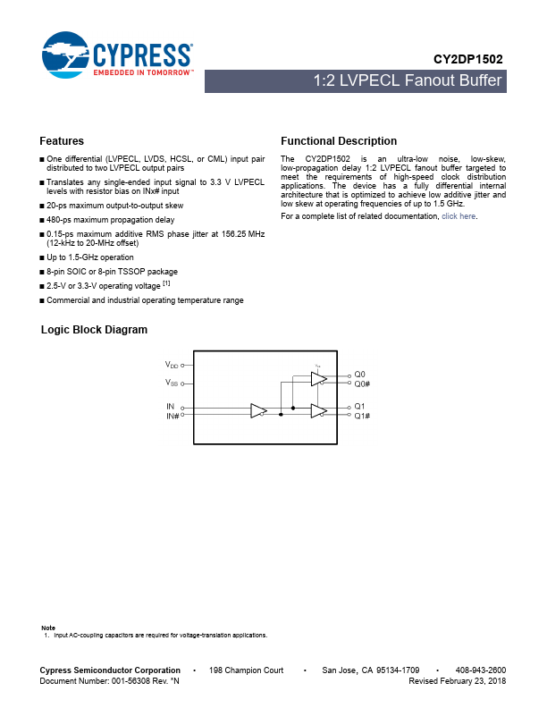
Functional Description
The CY2DP1502 is an ultra-low noise, low-skew, low-propagation delay 1:2 LVPECL fanout buffer targeted to meet the requirements of high-speed clock distribution applications. The device has a fully differential internal architecture that is optimized to achieve low additive jitter and low skew at operating frequencies of up to 1.5 GHz. For a plete list of related...