CY2DP314
CY2DP314 is 1 of 2:4 Differential Clock/Data Fanout Buffer manufactured by Cypress.
1 of 2:4 Differential Clock/Data Fanout Buffer
Features
- Four ECL/PECL differential outputs
- One ECL/PECL differential or single-ended inputs (CLKA)
- One HSTL differential or single-ended inputs (CLKB)
- Hot-swappable/-insertable
- 50-ps output-to-output skew
- 150-ps device-to-device skew
- 400-ps propagation delay (typical)
- 0.8-ps RMS period jitter (max.)
- 1.5-GHz operation (2.7-GHz maximum toggle frequency)
- PECL and HSTL mode supply range: VCC = 2.5V± 5% to 3.3V±5% with VEE = 0V
- ECL mode supply range: VE E =
- 2.5V± 5% to
- 3.3V±5% with VCC = 0V
- Industrial temperature range:
- 40°C to 85°C
- 20-pin SSOP package
- Temperature pensation like 100K ECL
Functional Description
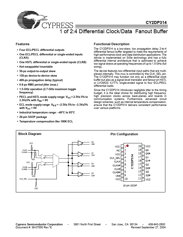
The CY2DP314 is a low-skew, low propagation delay 2-to-4 differential fanout buffer targeted to meet the requirements of high-performance clock and data distribution applications. The device is implemented on Si Ge technology and has a fully differential internal architecture that is optimized to achieve low signal skews at operating frequencies of up to 1.5 GHz (full swing). The device Features two differential input paths that are multiplexed internally. This mux is controlled by the CLK_SEL pin. The CY2DP314 may function not only as a differential clock buffer but also as a signal-level translator and fanout on HSTL or LVCMOS /LVTTL single-ended signal to four ECL/PECL differential loads. Since the CY2DP314 introduces negligible jitter to the timing budget, it is the ideal choice for distributing high frequency, high precision clocks across back-planes and boards in munication systems. Furthermore, advanced circuit design schemes, such as internal temperature pensation, ensure that the CY2DP314 delivers consistent performance over various platforms.
Block Diagram
VCC CLKA CLKA# Q0 Q0#
Pin Configuration
VCC NC VCC CLK_SEL CLKA CLKA# CLKB CLKB# VEE VCC
Q1 Q1# VEE
VCC CLKB CLKB#
Q2 Q2#
VEE CLK_SEL
Q3...