CY2DP818
CY2DP818 is 1:8 Clock Fanout Buffer manufactured by Cypress.
1:8 Clock Fanout Buffer
1:8 Clock Fanout Buffer
Features
- Low-voltage operation VDD = 3.3 V
- 1:8 fanout
- Operation to350 MHz
- Single input configurable for LVDS, LVPECL, or LVTTL
- 8 pair of LVPECL outputs
- Drives a 50 ohm load
- Low input capacitance
- Low output skew
- Low propagation delay (tpd = 4 ns, typical)
- Industrial temperature range
- 38-pin TSSOP Package
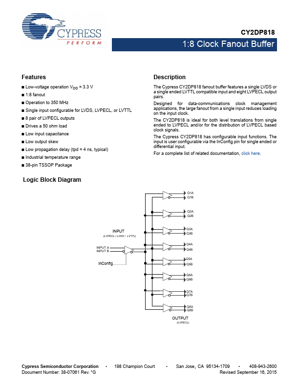
Logic Block Diagram
INPUT
(LVPECL / LVDS / LVTTL)
INPUT A INPUT B
In Config
Description
The Cypress CY2DP818 fanout buffer Features a single LVDS or a single ended LVTTL patible input and eight LVPECL output pairs. Designed for data-munications clock management applications, the large fanout from a single input reduces loading on the input clock. The CY2DP818 is ideal for both level translations from single ended to LVPECL and/or for the distribution of LVPECL based clock signals. The Cypress CY2DP818 has configurable input functions. The input is user configurable via the In...