CY2DP3110
CY2DP3110 is Differential Clock/Data Fanout Buffer manufactured by Cypress.
..
Fast Edge™ Series CY2DP3110
1 of 2:10 Differential Clock/Data Fanout Buffer
Features
- Ten ECL/PECL differential outputs
- One ECL/PECL differential or single-ended inputs (CLKA)
- One HSTL differential or single-ended inputs (CLKB)
- Hot-swappable/-insertable
- 50 ps output-to-output skew
- 150 ps device-to-device skew
- 400 ps propagation delay (typical)
- 1.2 ps RMS period jitter (max.)
- 1.5 GHz Operation (2.7 GHz maximum toggle frequency)
- PECL and HSTL mode supply range: VCC = 2.5V± 5% to 3.3V±5% with VEE = 0V
- ECL mode supply range: VE E =
- 2.5V± 5% to
- 3.3V±5% with VCC = 0V
- Industrial temperature range:
- 40°C to 85°C
- 32-pin TQFP package
- Temperature pensation like 100K ECL
- Pin-patible with MC100ES6111
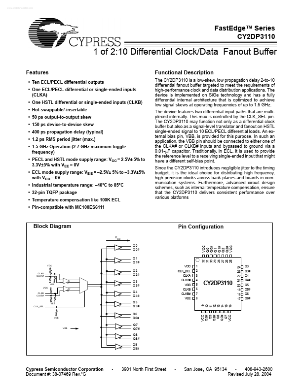
Functional Description
The CY2DP3110 is a low-skew, low propagation delay 2-to-10 differential fanout buffer targeted to meet the requirements of high-performance clock and data distribution applications. The device is implemented on Si Ge technology and has a fully differential internal architecture that is optimized to achieve low signal skews at operating frequencies of up to 1.5 GHz. The device Features two differential input paths that are multiplexed internally. This mux is controlled by the CLK_SEL pin. The CY2DP3110 may function not only as a differential clock buffer but also as a signal-level translator and fanout on HSTL single-ended signal to 10 ECL/PECL differential loads. An external bias pin, VBB, is provided for this purpose. In such an application, the VBB pin should be connected to either one of the CLKA# or CLKB# inputs and bypassed to ground via a 0.01-µF capacitor. Traditionally, in ECL, it is used to provide the reference level to a receiving single-ended input that might have a different self-bias point. Since the CY2DP3110 introduces negligible jitter to the timing budget, it is the ideal choice for distributing high frequency, high precision clocks across back-planes and boards in munication...