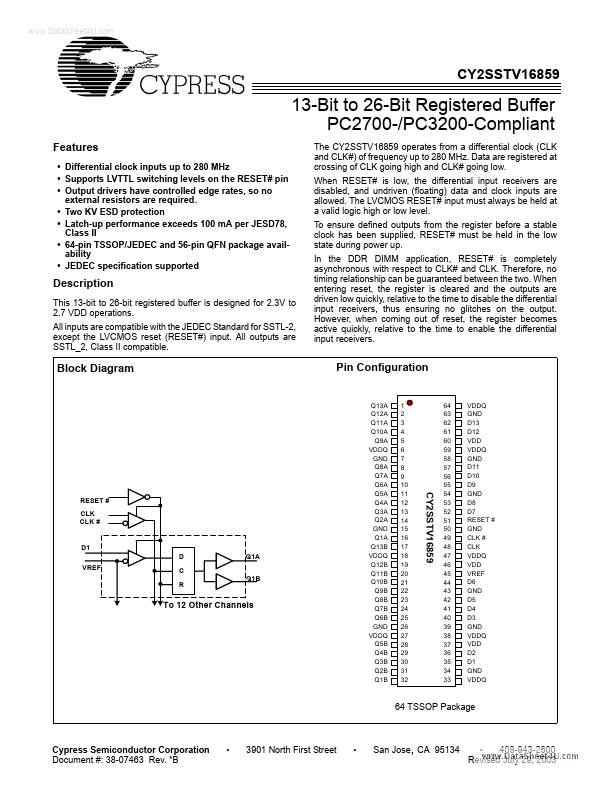
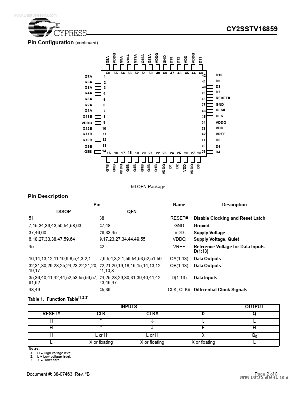
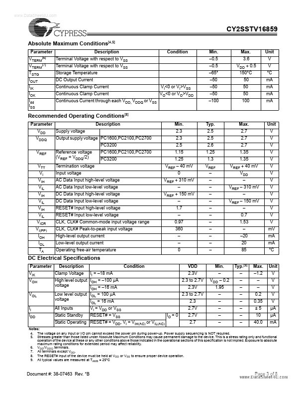
CY2SSTV16859 Description
This 13-bit to 26-bit registered buffer is designed for 2.3V to 2.7 VDD operations. All inputs are patible with the JEDEC Standard for SSTL-2, except the LVCMOS reset (RESET#) input. All outputs are SSTL_2, Class II patible.
CY2SSTV16859 Key Features
- Differential clock inputs up to 280 MHz
- Supports LVTTL switching levels on the RESET# pin
- Output drivers have controlled edge rates, so no external resistors are required
- Two KV ESD protection
- Latch-up performance exceeds 100 mA per JESD78, Class II
- 64-pin TSSOP/JEDEC and 56-pin QFN package availability
- JEDEC specification supported The CY2SSTV16859 operates from a differential clock (CLK and CLK#) of frequency up to 280