CY2SSTV16859
CY2SSTV16859 is 13-Bit to 26-Bit Registered Buffer manufactured by SpectraLinear.
13-Bit to 26-Bit Registered Buffer PC2700-/PC3200-pliant
Features
- Differential clock inputs up to 280 MHz
- Supports LVTTL switching levels on the RESET# pin
- Output drivers have controlled edge rates, so no external resistors are required.
..
The CY2SSTV16859 operates from a differential clock (CLK and CLK#) of frequency up to 280 MHz. Data are registered at crossing of CLK going high and CLK# going low. When RESET# is low, the differential input receivers are disabled, and undriven (floating) data and clock inputs are allowed. The LVCMOS RESET# input must always be held at a valid logic high or low level. To ensure defined outputs from the register before a stable clock has been supplied, RESET# must be held in the low state during power up. In the DDR DIMM application, RESET# is pletely asynchronous with respect to CLK# and CLK. Therefore, no timing relationship can be guaranteed between the two. When entering reset, the register is cleared and the outputs are driven low quickly, relative to the time to disable the differential input receivers, thus ensuring no glitches on the output. However, when ing out of reset, the register bees active quickly, relative to the time to enable the differential input receivers.
- Two KV ESD protection
- Latch-up performance exceeds 100 m A per JESD78, Class II
- 64-pin TSSOP/JEDEC and 56-pin QFN package availability
- JEDEC specification supported
Description
This 13-bit to 26-bit registered buffer is designed for 2.3V to 2.7 VDD operations. All inputs are patible with the JEDEC Standard for SSTL-2, except the LVCMOS reset (RESET#) input. All outputs are SSTL_2, Class II patible.
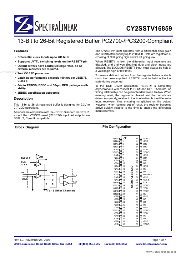
Block Diagram
Pin Configuration
RESET # CLK CLK #
D1 D VREF C Q1B R Q1A
To 12 Other Channels
Q13A Q12A Q11A Q10A Q9A VDDQ GND Q8A Q7A Q6A Q5A Q4A Q3A Q2A GND Q1A Q13B VDDQ Q12B Q11B Q10B Q9B Q8B Q7B Q6B GND VDDQ Q5B Q4B Q3B Q2B Q1B
1 2 3 4 5 6 7 8 9 10 11 12 13 14 15 16 17 18 19 20 21 22 23...